Borophosphosilicate glass incorporated with fluorine for low thermal budget gap fill

a technology of borophosphosilicate glass and fluorine, which is applied in the manufacturing of semiconductor/solid-state devices, basic electric elements, electric devices, etc., can solve the problems of reducing the viscosity of bpsg, limiting the concentration of boron and phosphorus, and imposing severe restrictions on the time, temperature and atmosphere of all thermal process steps. , to achieve the effect of enhancing the gap filling capability

Inactive Publication Date: 2000-12-12
IBM CORP
View PDF16 Cites 16 Cited by
  • Summary
  • Abstract
  • Description
  • Claims
  • Application Information

AI Technical Summary

Benefits of technology

is to provide a method of forming a borophosphosilicate glass with enhanced gap fill capability to provide a void free fill of structures with aspect ratios greater than 6:1.

Problems solved by technology

Advanced semiconductor devices, such as highly dense dynamic random access memories (DRAMs) or logic chips, impose severe restrictions on the times, temperatures, and atmospheres of all thermal process steps.
The viscosity of the BPSG can be decreased by increasing the reflow temperature, which is undesirable, or by increasing the dopant concentrations of boron and phosphorus in the BPSG.
However, the dopant concentrations for boron and phosphorus are limited to about 5 weight percent each since exceeding this concentration results in surface crystal growth of boric acid or boric phosphate after deposition.
Surface crystals are not desirable due to fabrication integration problems with subsequent lithography, reactive ion etching and chemical mechanical polishing processes.
Furthermore, increasing dopant concentrations lead to hygroscopic films.

Method used


Image

  • Borophosphosilicate glass incorporated with fluorine for low thermal budget gap fill
  • Borophosphosilicate glass incorporated with fluorine for low thermal budget gap fill
  • Borophosphosilicate glass incorporated with fluorine for low thermal budget gap fill

Examples


example

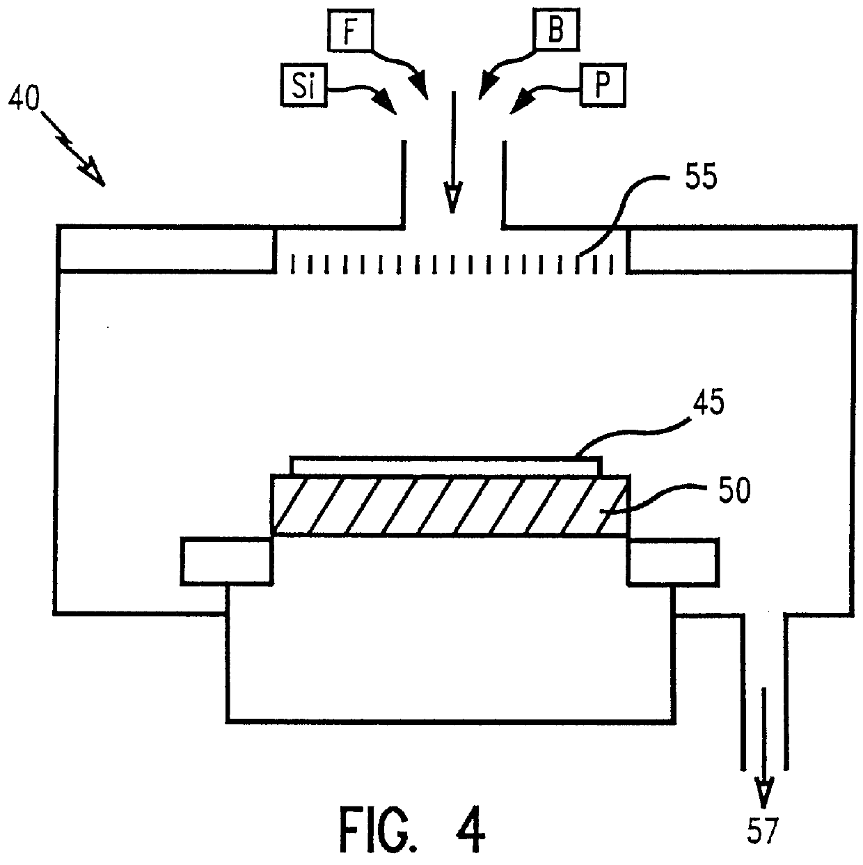
FBPSG films of the present invention were produced in accordance with the first embodiment of the aforementioned process in a chemical vapor deposition chamber, specifically, an Applied Materials P5000 SABPSG reactor. The following tables show the results of the gap fill for as-deposited and annealed films comparing the prior art BPSG films with the FBPSG films of the present invention.

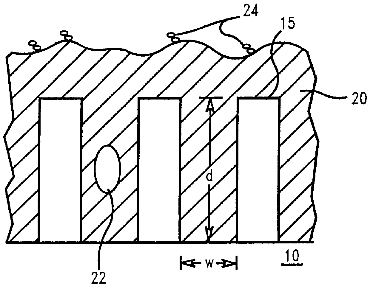
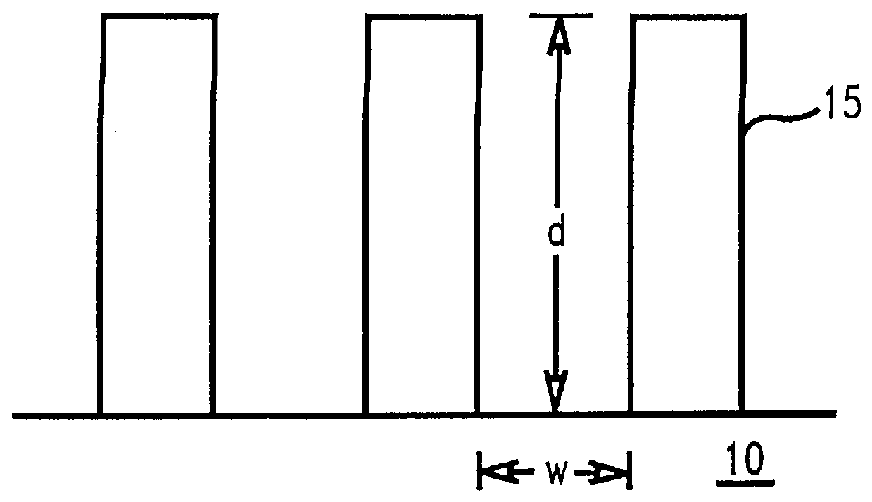
Semiconductor wafers with gaps having aspect ratios of about 1:1 and a width of about 0.3 .mu.m were used to compare the quality of an as-deposited prior art BPSG film and an as-deposited FBPSG film of the present invention. Deposition of the films occurred at 480.degree. C. at a sub-atmospheric pressure of about 200 Torr.

The prior art BPSG film showed significant voids in the as-deposited film whereas the FBPSG film was substantially void-free.

Semiconductor wafers with gaps having aspect ratios of about 8:1 and widths of about 0.04 .mu.m were used to compare the quality of a prior art BPSG film and a...


PUM


Abstract

A method of depositing a fluorinated borophosphosilicate glass (FBPSG) on a semiconductor device as either a final or interlayer dielectric film. Gaps having aspect ratios greater than 6:1 are filled with a substantially void-free FBPSG film at a temperature of about 480 DEG C. at sub-atmospheric pressures of about 200 Torr. Preferably, gaseous reactants used in the method comprise TEOS, FTES, TEPO and TEB with an ozone/oxygen mixture. Dopant concentrations of boron and phosphorus are sufficiently low such that surface crystallite defects and hygroscopicity are avoided. The as-deposited films at lower aspect ratio gaps are substantially void-free such that subsequent anneal of the film is not required. Films deposited into higher aspect ratio gaps are annealed at or below about 750 DEG C., well within the thermal budget for most DRAM, logic and merged logic-DRAM chips. The resultant FBPSG layer contains less than or equal to about 5.0 wt % boron, less than about 4.0 wt % phosphorus, and about 0.1 to 2.0 wt % fluorine.

Description

1. Field of the InventionThis invention relates to a method of manufacturing a semiconductor device and, in particular, to a method of forming a low temperature, low viscosity, fluorinated borophosphosilicate glass (FBPSG) layer on the device.2. Description of Related ArtIn the manufacture of semiconductor electronic components, it is necessary to encapsulate the component in a glass or to use glass as an interlayer dielectric film. Typically, the glass layer is a SiO.sub.2 layer which is formed on the surface of the component using chemical vapor deposition (CVD). As a result of increasing demands in industry, the need for finer circuitry patterns and increased circuit density have made it necessary to develop improved glass layers for layering the semiconductor surfaces during the fabrication process. Advanced semiconductor devices, such as highly dense dynamic random access memories (DRAMs) or logic chips, impose severe restrictions on the times, temperatures, and atmospheres of ...

Claims


Application Information

Patent Timeline
Patent Type & Authority Patents(United States)
IPC IPC(8): H01L21/02H01L21/316H01L21/20
CPCH01L21/31604H01L21/31629H01L21/31625H01L21/02129H01L21/02131H01L21/02214H01L21/02271H01L21/3105H01L21/20H01L21/02205H01L21/02211H01L21/02216H01L21/02274
Inventor CHAKRAVARTI, ASHIMA B.CONTI, RICHARD A.LIUCCI, FRANK V.RESTAINO, DARRYL D.
Owner IBM CORP
Why Eureka
Try Eureka