Method for manufacturing a micromechanical relay

a micro-mechanical relay and manufacturing method technology, applied in the direction of piezoelectric/electrostrictive devices, decorative arts, chemical vapor deposition coating, etc., can solve the problems of two chips, very expensive and difficult so-called chip bonding, and metal structure must be very thin

Inactive Publication Date: 2000-12-19
FRAUNHOFER GESELLSCHAFT ZUR FOERDERUNG DER ANGEWANDTEN FORSCHUNG EV
View PDF12 Cites 117 Cited by
  • Summary
  • Abstract
  • Description
  • Claims
  • Application Information

AI Technical Summary

Problems solved by technology

The connection of the two chips, the so-called chip bonding is, however, very expensive and difficult.
This has, however, the disadvantage that this metal structure must be very thin so as to reduce the thermostatic bimetal effect between the supporting beam and the conductor path.
One the one hand, sticking can occur during the production of an electrostatically actuated micromechanical relay and, on the other hand, it can occur during operation of said relay.
It is also possible that the restoring forces of the beam deteriorate due to material fatigue during the service life so that permanent sticking of the structure to the substrate may occur as a result: of such reduced restoring forces.

Method used


Image

  • Method for manufacturing a micromechanical relay
  • Method for manufacturing a micromechanical relay
  • Method for manufacturing a micromechanical relay

Examples


second embodiment

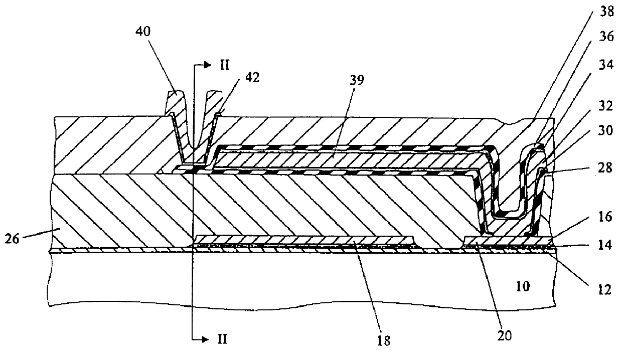
FIGS. 10a and 10b show sectional side views of the layer structure before and after the removal of the sacrificial layer; these sectional side views serve to illustrate a second preferred embodiment of the present invention. The second preferred embodiment differs from the first preferred embodiment essentially with regard to the formation of the anchoring region of the beam structure on the substrate. The above-described configurations of the beam structure and the described methods for etching the sacrificial layer can also be used for the

A substrate 100 is again used as a base material, said substrate 100 being once more a silicon wafer in this embodiment. In the present embodiment, the substrate 100 is doped so as to define a fixed electrode. The substrate can be doped over the full area or partially. Subsequently, the substrate 100 has applied thereto an insulating layer 12, e.g. SiO.sub.2.

Following this, the resultant structure has applied thereto a sacrificial layer or spacin...

first embodiment

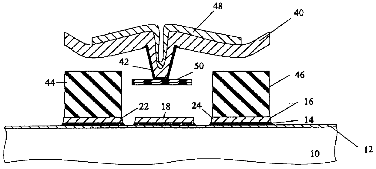
The sacrificial layer 126 of this embodiment has now applied thereto the composite layer structure which has been described with reference to the The composite layer structure is then structured, e.g. photolithographically, so as to define the beam structure and, in addition, the two contacts to be closed by the relay; in FIGS. 10a and 10b only one of said contacts, viz. contact 144, is shown. During or after said structuring, the upper passivation layer and the upper adhesive layer are removed from the contacts. Following this, a contact area in the form of a contact bridge 140 is formed by means of photolithographic processes, e.g. by making use of a mask 130, said contact bridge 140 being formed on the subsequently movable end of the beam structure, such that it is insulated from said beam structure; at least part of the bottom side of the contact bridge has again arranged thereon an adhesive layer 142.

Following this, the mask 130 is removed and the sacrificial layer is etched i...


PUM

PropertyMeasurementUnit
areaaaaaaaaaaa
sizeaaaaaaaaaa
conductiveaaaaaaaaaa

Abstract

PCT No. PCT/EP97/06174 Sec. 371 Date May 11, 1999 Sec. 102(e) Date May 11, 1999 PCT Filed Nov. 6, 1997 PCT Pub. No. WO98/21734 PCT Pub. Date May 22, 1998A method of producing a micromechanical relay comprises the steps of providing a substrate including a conductive fixed electrode in or on said substrate. A sacrificial layer and a conductive layer are applied and the conductive layer is structured so as to define a beam structure as a movable counterelectrode opposite said fixed electrode. A contact area is applied, the conductive layer extending between an anchoring region and the contact area and being insulated from said contact area. Subsequently, the sacrificial layer is removed by means of etching so as to produce the beam structure comprising a movable area and an area secured to the anchoring region on the substrate. The beam structure is defined such that etch access openings in said beam structure are structured such that the size of the area covered by the etch access openings used for etching the sacrificial layer increases from the area of the beam structure secured to the substrate to the movable area of the beam structure so that the etching of the sacrificial layer is controlled in such a way that the portion of the sacrificial layer arranged below the movable area of the beam structure is etched faster than the portion of the sacrificial layer arranged in the area of the anchoring region.

Description

1. Field of the InventionThe present invention refers to a method of producing a micromechanical relay.2. Description of Prior ArtA relay fundamentally serves to switch electric currents. Since the switching of electric currents often has to be accomplished in the field of technology, there is a large field of application for relays. Recently, micromechanical relays have been developed, which, due to the use of semiconductor technology, are based on a new electrostatic principle of action.This electrostatic principle of action permits an almost powerless switching of currents. This property is of importance especially in cases of use where a connection to the electric mains is not possible, i.e. in cases of use where power is supplied by a battery. Such use becomes increasingly common, e.g. in wireless transmission in the field of communication technology. In order to guarantee here a sufficiently long operating time, it is important to keep power consumption low. A micromechanical ...

Claims


Application Information

Patent Timeline
Patent Type & Authority Patents(United States)
IPC IPC(8): B81B3/00H01H59/00B81C1/00
CPCB81C1/00936H01H59/0009B81B2201/018H01H2059/0072H01H2059/0018
Inventor SCHIELE, IGNAZKOZLOWSKI, FRANK
Owner FRAUNHOFER GESELLSCHAFT ZUR FOERDERUNG DER ANGEWANDTEN FORSCHUNG EV
Why Eureka
Try Eureka