Semiconductor devices

a technology of semiconductors and display devices, applied in the direction of radio frequency controlled devices, optics, instruments, etc., can solve the problems of increasing resistance, affecting the reliability of the device,

Inactive Publication Date: 2000-12-26
SEMICON ENERGY LAB CO LTD
View PDF5 Cites 165 Cited by
  • Summary
  • Abstract
  • Description
  • Claims
  • Application Information

AI Technical Summary

Problems solved by technology

If, however, narrow conductor lines are used, problems arising from their increased resistances will become evident.
Such a construction is not preferable though because it complicates processing steps needed for the production of the active matrix LCD device.
However, the use of al

Method used


Image

  • Semiconductor devices
  • Semiconductor devices
  • Semiconductor devices

Examples


first embodiment

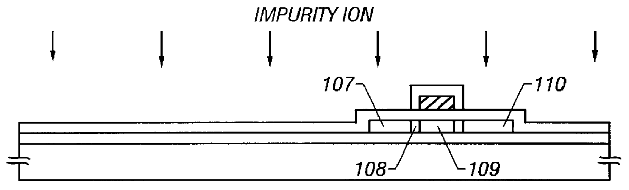
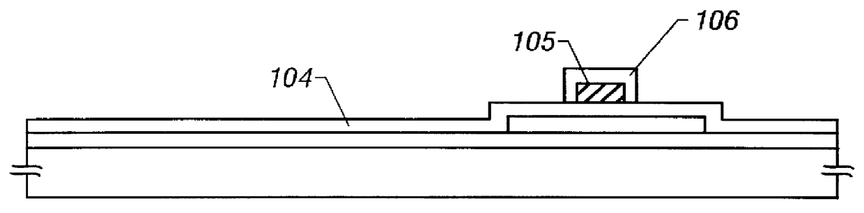
FIGS. 1 and 2 generally illustrate successive processing steps for the production of an active matrix LCD device according to the present invention. First, silicon dioxide is coated to a thickness of 3000 .ANG. on a substrate 101 which is constructed with a sheet of glass or quartz to form an undercoat 102 thereupon. This undercoat 102 may be formed by a plasma chemical vapor deposition (CVD) process or a sputtering process.

The silicon dioxide undercoat 102 helps suppress diffusion of impurities from the substrate 101 and make mechanical stresses occurring between the substrate 101 and a later-produced semiconductor layer less severe. When a sheet of quartz is used as the substrate 101, it is preferable to produce a thick anodic oxidization film which forms the undercoat 102. This is because the quartz substrate shrinks much less than the silicon dioxide undercoat 102 when heated so that stresses are likely to occur between the substrate 101 and the semiconductor layer.

After the und...

second embodiment

The second embodiment of the invention features a different construction of gate electrodes in comparison with the first embodiment. More particularly, each gate electrode is formed in a three-layer structure including a titanium film, an aluminum film and another titanium film.

FIGS. 4(A)-(D) illustrate how a gate electrode of the second embodiment is produced. Shown in FIG. 4(A) is an unfinished gate electrode which has been produced by forming a titanium film 402 to a thickness of about 100 .ANG. on top of a gate insulation layer 401, a aluminum film 403 containing a small amount of scandium to a thickness of 5000 .ANG. on top of the titanium film 402, and a titanium film 404 to a thickness of about 100 .ANG. on top of the aluminum film 403, and then patterning this three-layer structure of the titanium film 402, aluminum film 403 and titanium film 404 to the shape of a gate electrode.

After the structure shown in FIG. 4(A) has been obtained, it is subjected to an anodic oxidizatio...


PUM


Abstract

In an active matrix liquid crystal display (LCD) device, a conductor line interconnecting a drain of each thin-film transistor and a corresponding pixel electrode constructed with indium tin oxide (ITO) is formed in a three-layer structure in which an aluminum film is sandwiched between a pair of titanium films. This construction prevents poor contact and deterioration of reliability because electrical contact is established between one titanium film and semiconductor and between the other titanium film and ITO. The aluminum film has low resistance which is essential for ensuring high performance especially in large-screen LCDs.

Description

1. Field of the InventionThe present invention relates to the construction of an active matrix display device such as an active matrix liquid crystal display (LCD) device.2. Description of the Related ArtIn an active matrix LCD device, thin-film transistors are arranged on a sheet of quartz or glass at a high density. It is increasingly required in recent years to raise the level of integration of the thin-film transistors. On the other hand, it is more and more required for the LCD device to provide larger display areas to meet the growing demand for large-screen displays. This is where the LCD device greatly differs from large-scale integrated (LSI) circuits which are required to provide higher integration levels and smaller physical sizes.Besides the requirement for large-screen display, it is desired to make the conductor lines of the LCD device as narrow as possible so as to provide an increased aperture ratio. If, however, narrow conductor lines are used, problems arising from...

Claims


Application Information

Patent Timeline
IPC IPC(8): G02F1/13G02F1/1362H01L21/02H01L27/12H01L21/336G02F1/1335H01L21/28G02F1/1343G02F1/1368H01L21/3205H01L23/52H01L29/786
CPCG02F1/136286H01L29/66757H01L27/12G02F2001/13629G02F1/13629H01L29/786
Inventor YAMAZAKI, SHUNPEI
Owner SEMICON ENERGY LAB CO LTD
Why Eureka
Try Eureka