High speed low skew CMOS to ECL converter

a converter and low skew technology, applied in the field of circuits, can solve problems such as significant operational errors, and unfavorable unexpected changes in logic values

Inactive Publication Date: 2001-01-16
SEMICON COMPONENTS IND LLC
View PDF19 Cites 6 Cited by
  • Summary
  • Abstract
  • Description
  • Claims
  • Application Information

AI Technical Summary

Benefits of technology

The first and second switches of the first branch are preferably formed of an inverter that is essentially the only delay component associated with the converter of the present invention. In effect, logic level translations are achieved within one gate delay. That shortest delay possible for a logic level converter, and the mirroring of the designs of the potential drop components in the respective branches, results in minimum propagation delay, very low skew for low-to-high and high-to-low transitions, and minimum pulse width distortion. Both branches share any potential deviations that could be caused by fabrication, temperature, and / or Vcc variations equally such that the desired potential differential will remain substantially constant.

Problems solved by technology

Furthermore, minor potential swings in CMOS signals may not effect any logic level change therein; however, they may be significant enough to cause an unexpected change in a TTL or an ECL logic value when transmitted to a TTL-or an ECL-based system.
Clearly, unexpected changes in logic values are not desirable.
They can cause significant operational errors.
This problem is more likely to occur as transmission rates are increased.
However, the gain in increased transmission rate is often undermined by an increase in signal noise.
When the wider-swing CMOS logic systems interface with smaller-swing bipolar-transistor-based logic systems the noise associated with CMOS operation may generate enough of a swing to cause an undesired transistor switching.
The signal bounce that occurs with the rapid switching often creates reflections in transmission media.
However, efforts to minimize distortions can result in increased signal propagation delays--an undesirable condition in smaller, faster systems.
To that end, they subject both signals to undesirable distortions that can occur during signal transitions.
In addition, the Lam converter is referenced to the high-potential power rail and more susceptible to temperature, fabrication, and Vcc changes affecting signal amplitude and transmission rate.
An added branch such as this increases the size of the converter--an undesirable prospect when smaller devices are of importance.

Method used


Image

  • High speed low skew CMOS to ECL converter
  • High speed low skew CMOS to ECL converter
  • High speed low skew CMOS to ECL converter

Examples


Embodiment Construction

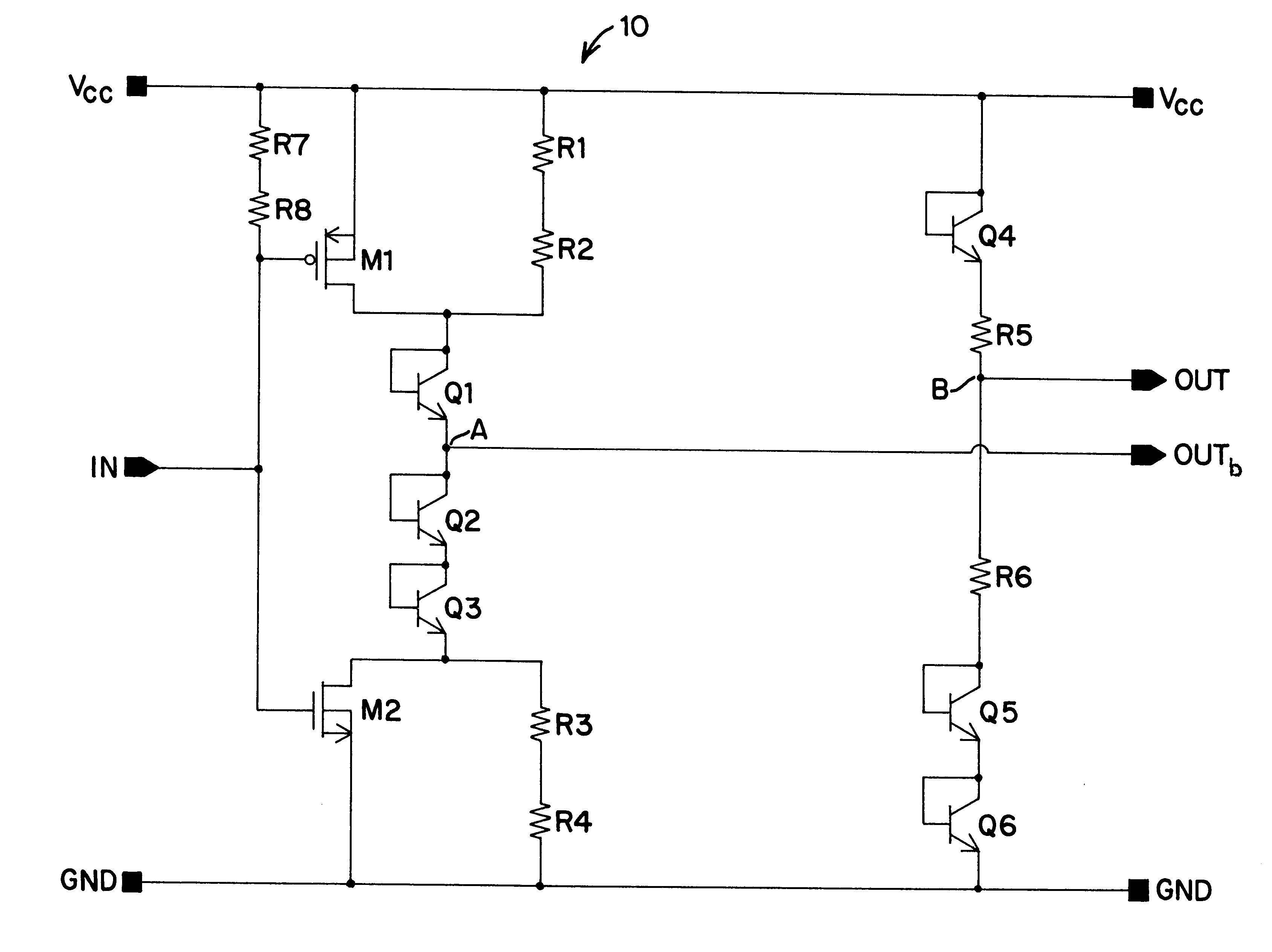
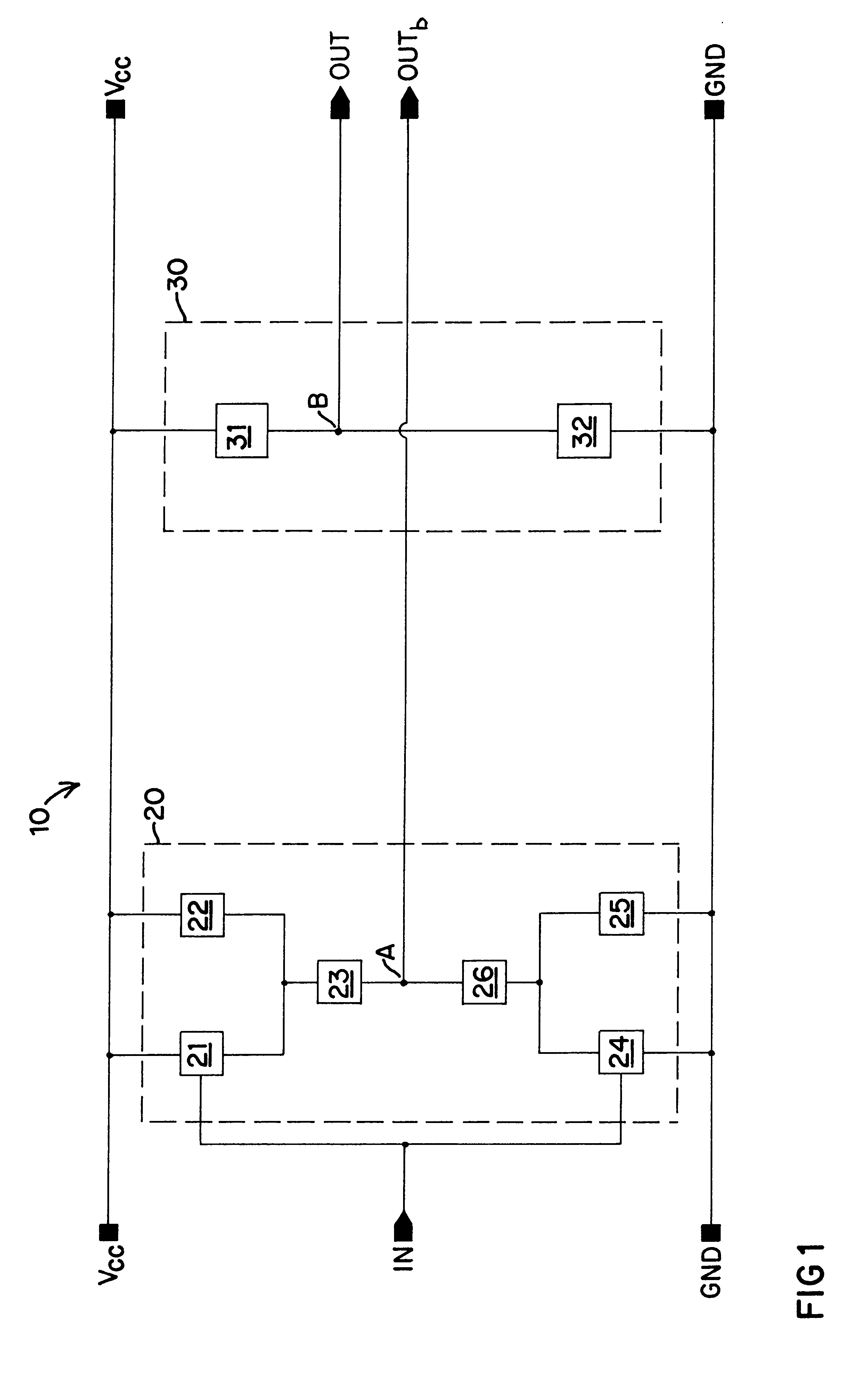
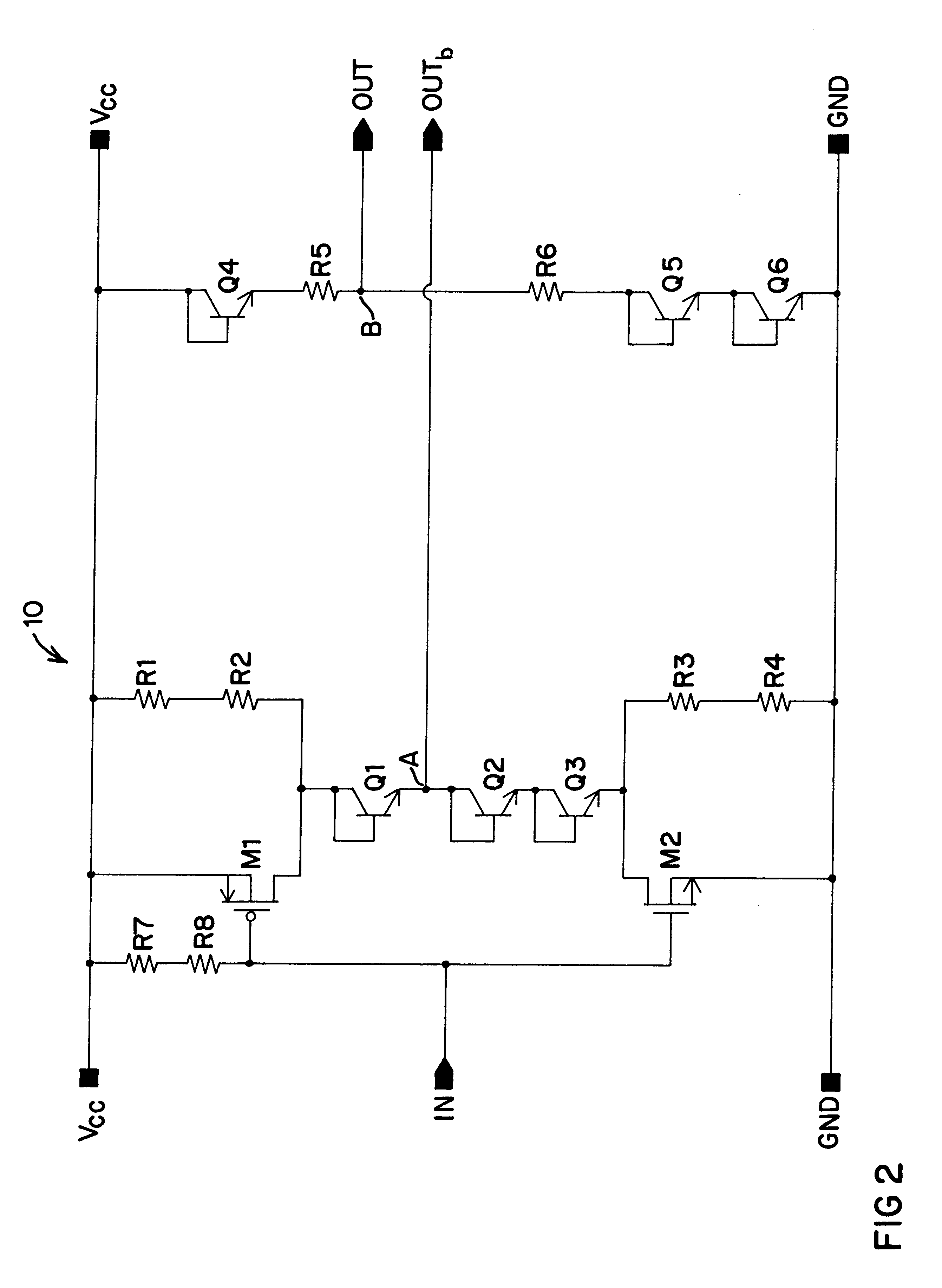
A high speed, low skew, logic level converter 10 of the present invention is shown in simplified form in FIG. 1. The converter 10 is designed to translate a single switching signal at input node IN from a potential associated with CMOS logic levels into a complementary pair of output signals at OUT and OUTb that are at potentials associated with ECL logic levels. It is contemplated that the potentials associated with OUT and OUTb may be developed by the converter 10 at levels other than those related to ECL including, but not limited to Gunning Transceiver Logic (GTL).

The converter 10 of the present invention includes a first converter branch 20 and a second converter branch 30, wherein output node OUTb is coupled to first converter branch 20 and output node OUT is coupled to second converter branch 30. It is to be noted that input node IN is coupled only to first converter branch 20 and therefore only controls the operation of that branch. On the other hand, second branch 30 is not...


PUM


Abstract

A logic level converter for translating CMOS logic signals to into differential logic signal pairs such as those associated with ECL levels. The converter includes a first converter branch coupled to the switchable CMOS level input and it provides a first switchable translated output. A second converter branch is not coupled to the input nor is it coupled to the first converter branch. The second converter branch provides a fixed reference signal output around which the output of the first converter branch switches. Changes in the input signal to the first converter branch cause its output potential to be more than or less than the potential of the fixed reference signal supplied by the second converter branch. The components of the respective branches may be tailored to position the fixed signal at a selectable level and to define the differential between the two output signals. The current associated with the converter is mirrored through both branches to minimize the effects of fabrication, temperature, and / or power supply vagaries.

Description

1. Field of the InventionThe present invention relates to circuitry for transmitting electrical signals from one location to another. In particular, the present invention relates to converters for changing the logic levels associated with the operation of Complementary Metal-Oxide-Silicon (CMOS) transistors to the logic levels associated with the operation of emitter-coupled logic (ECL) transistors.2. Description of the Prior ArtA voltage level converter is used to adjust the logic high and logic low voltage levels associated with a single input signal, or a pair of input signals, coming into the converter to high and low voltage levels compatible with downstream circuitry. The converter must transfer these electrical signals at desired amplitude and rate. The signal transfer occurs between active devices that are either on the same semiconductor-based chip or on different chips. The devices may be located proximate to one another, or they may be some distance from one another. One ...

Claims


Application Information

Patent Timeline
IPC IPC(8): H03K19/003H03K19/0175
CPCH03K19/00376H03K19/017527E02D27/28E02D5/808E02D2250/0007E02D2250/0023
Inventor GOODELL, TRENOR F.
Owner SEMICON COMPONENTS IND LLC
Why Eureka
Try Eureka