Aluminum metallization by a barrier metal process

a technology of barrier metal and aluminum, which is applied in the direction of semiconductor devices, electrical equipment, semiconductor/solid-state device details, etc., can solve the problems of inferior smoothness of the ti layer formed directly on the surface of e.g. a silicon substrate, and achieve superior step coverage characteristics, high reliability and reproducibility, and superior barrier characteristics

Inactive Publication Date: 2001-03-06
SONY CORP
View PDF14 Cites 10 Cited by
  • Summary
  • Abstract
  • Description
  • Claims
  • Application Information

AI Technical Summary

Benefits of technology

It is seen from above that superior barrier characteristics may be achieved by the present invention by the three-layer barrier metal structure while superior step coverage characteristics may also be achieved by the Ti layer provided in the interface region adjacent to the layer of the Al-based material. The contact holes can be filled with the Al-based material with high reliability and re

Problems solved by technology

However, this Ti layer partially reflects the rough surface morphology associated with the columnar crystal structure of the under

Method used


Image

  • Aluminum metallization by a barrier metal process
  • Aluminum metallization by a barrier metal process
  • Aluminum metallization by a barrier metal process

Examples


example 2

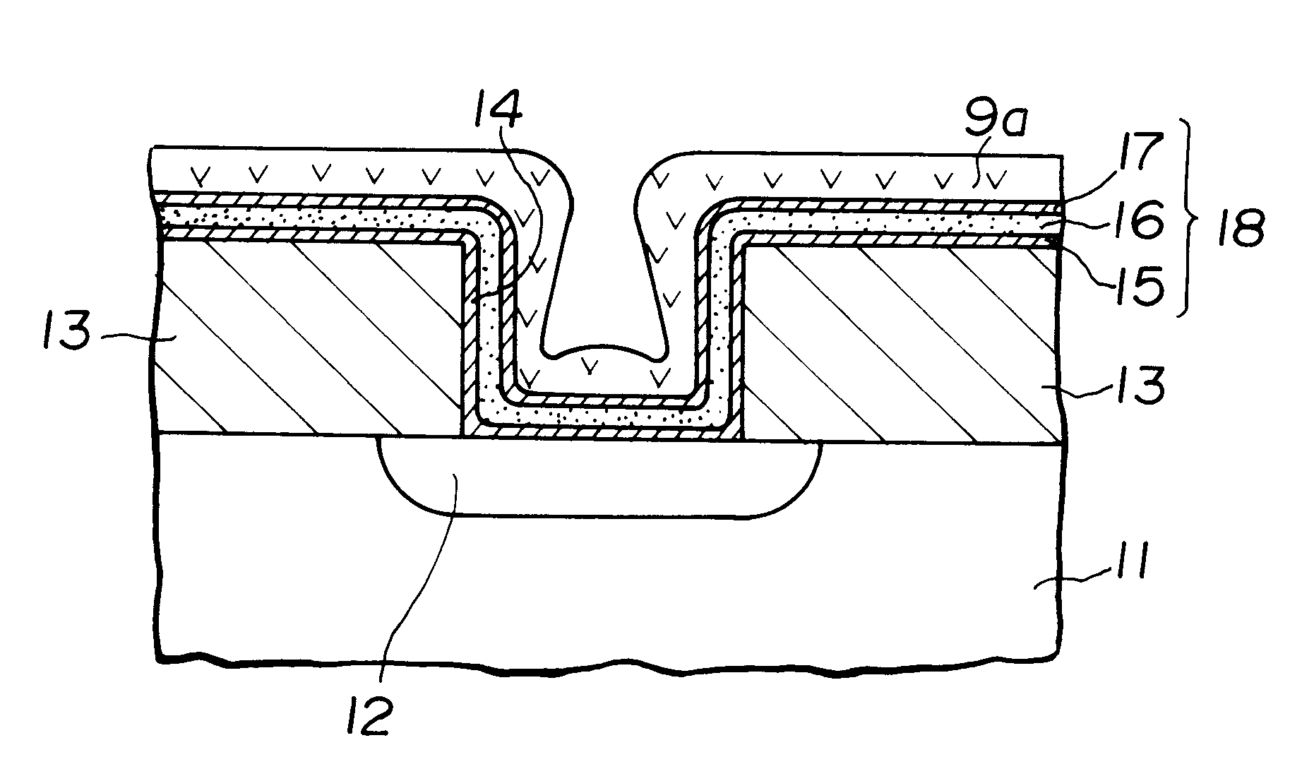
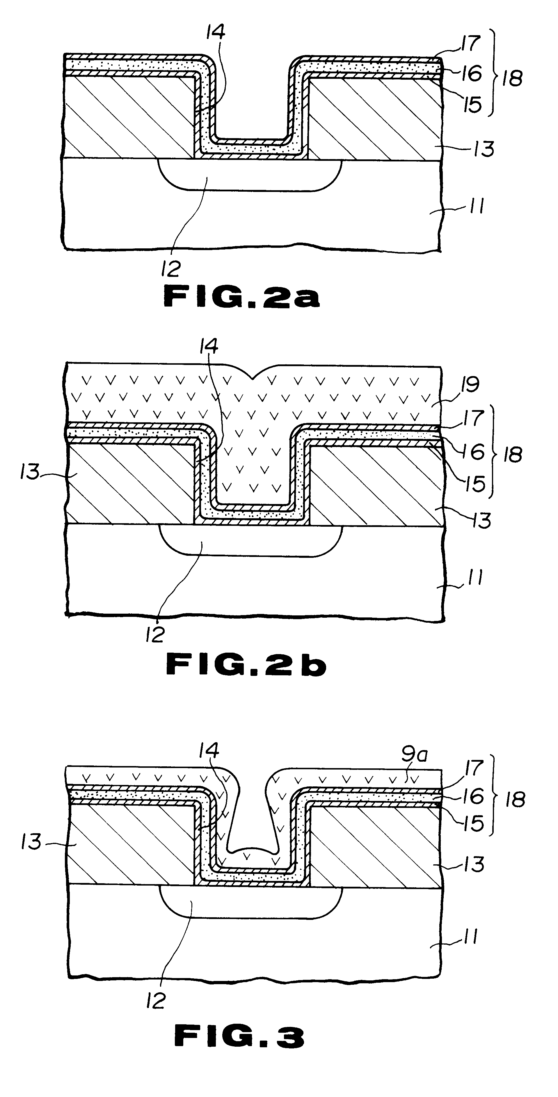
In the present example, the Al-1% Si alloy was buried in the contact hole by two-stage sputtering. This process is explained by referring to FIGS. 2a and 2b and also to FIG. 3.

A wafer similar to that used in FIG. 2a was prepared and subjected to a first-stage sputtering under typical operating conditions of an Ar flow rate of 100 SCCM, a gas pressure of 0.47 Pa (3.5 mTorr), a d.c. sputtering power of 22.5 kW, an RF bias voltage of 0 volts, a sputtering time of 5 seconds and a sputtering rate of 1.2 .mu.m / minute, without heating the substrate. As a result, a first Al-1% Si layer 9a having a thickness of approximately 100 nm was conformally formed after the pattern of the contact hole 14, as shown in FIG. 3.

Then, as a second stage sputtering, the reverse side of the substrate was contacted with a hot Ar gas for heating the substrate to about 500.degree. C., and high temperature bias sputtering was carried out under operating conditions of a d.c. sputtering power of 10.5 kW, an RF bias...


PUM


Abstract

A metallization method for filling an Al-based material in a contact hole having a barrier metal structure, in which high barrier characteristics and high step coverage may be achieved simultaneously, is proposed. The present invention is based on two concepts. The first concept is to provide a Ti/TiON/Ti three-layer barrier metal structure and to deposit a layer of the Al-based material by high temperature sputtering. Sufficient barrier characteristics may be provided by the intermediate TiON layer of the three-layer structure. The interface between the Al-based layer and the barrier metal layer is the Ti layer having excellent wetting characteristics with respect to the Al-based layer so that the contact hole can be filled uniformly without forming voids. The second concept is to set the substrate heating temperature during high temperature sputtering to 450 to 550° C. and to set the deposition rate to 0.6 mum/minute or less. In this manner, moderate Al migration and sufficiently long reaction time may be assured even on a Ti layer which partially reflects the rough surface morphology of the TiON layer for further improving reliability in filling.

Description

1. Field of the InventionThis invention relates to a method for metallization in the preparation of semiconductor devices. More particularly, it relates to a method for aluminum metallization for uniformly burying an aluminum-based material in a contact section having a barrier metal structure.2. Description of Related ArtIn keeping up with an increasing refinement of the design rule for semiconductor devices, as exemplified by VLSIs or ULSIs of recent origin, the contact hole formed in an interlayer insulating film for establishing electrical an connection between an upper metallization and a lower metallization is becoming increasingly smaller in diameter, such that the aspect ratio now exceeds unity. The upper metallization is usually formed by depositing an Al-based material by sputtering. However, it is difficult with this method to achieve sufficient step coverage to fill the contact hole having such a high aspect ratio so that a disconnection is frequently produced.Recently, ...

Claims


Application Information

Patent Timeline
IPC IPC(8): H01L21/768H01L21/70H01L23/48H01L23/485H01L23/52H01L23/532
CPCH01L21/76843H01L21/76877H01L21/76882H01L23/485H01L23/53223H01L2924/0002H01L2924/00
Inventor TAGUCHI, MITSURUKOYAMA, KAZUHIDE
Owner SONY CORP
Why Eureka
Try Eureka