

Method of plasma etching the tungsten silicide layer in the gate conductor stack formation
a technology of tungsten silicide layer and gate conductor, which is applied in the manufacture of basic electric elements, electric devices, semiconductor/solid-state devices, etc., can solve the problems of unsatisfactory value for subsequent processing steps, and achieve the effect of improving device quality factors
- Summary
- Abstract
- Description
- Claims
- Application Information
AI Technical Summary
Benefits of technology
Problems solved by technology
Method used
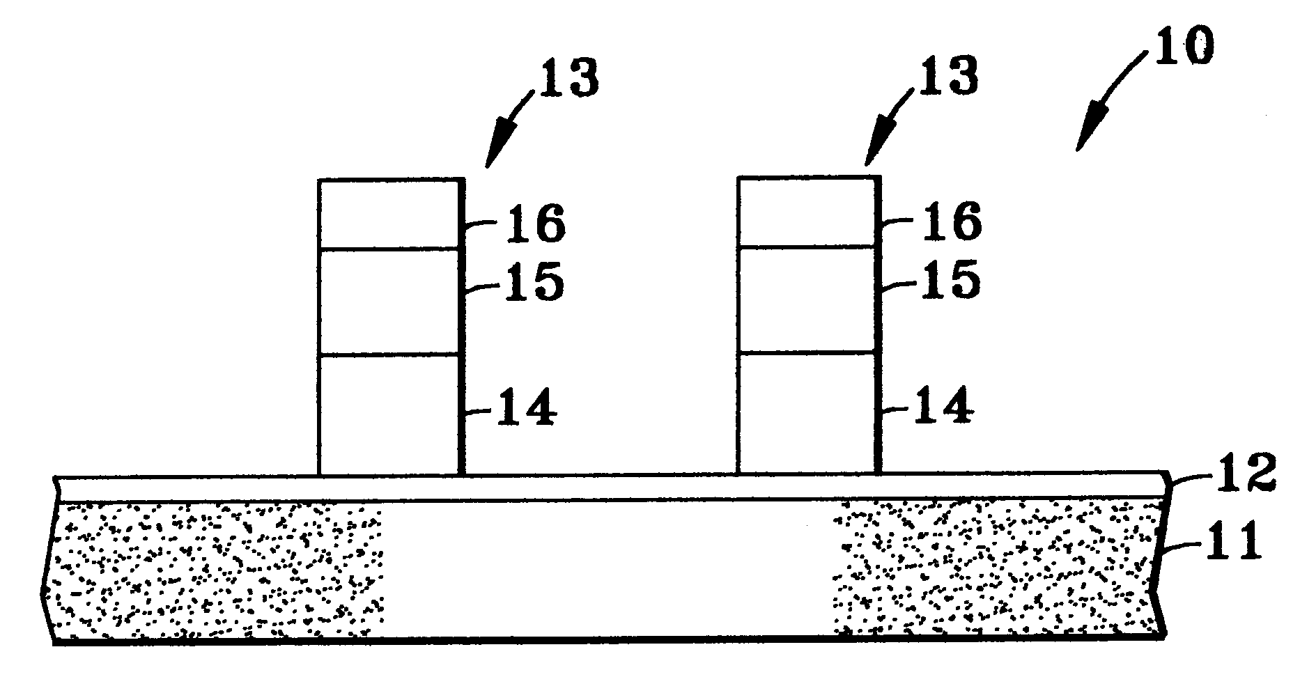
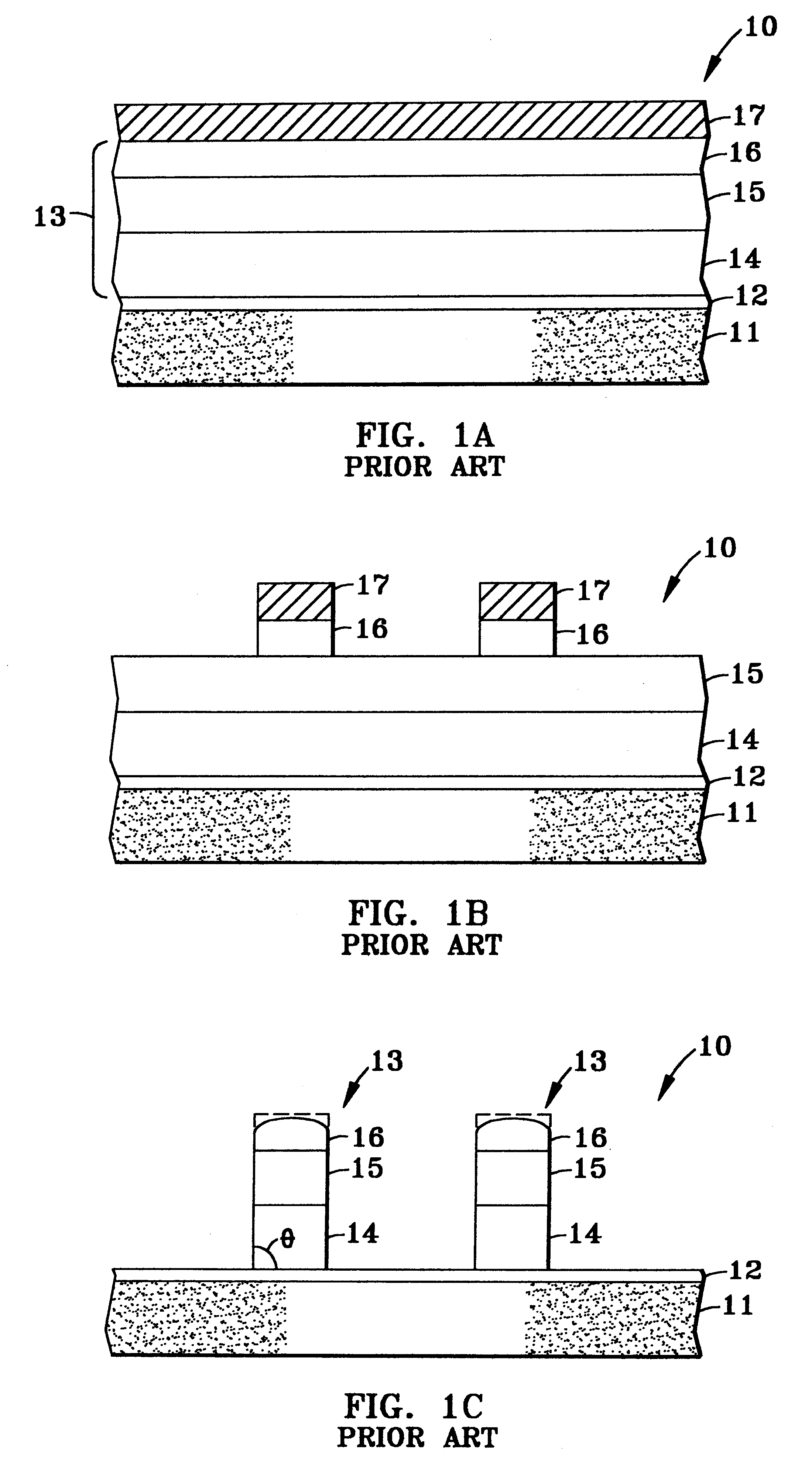
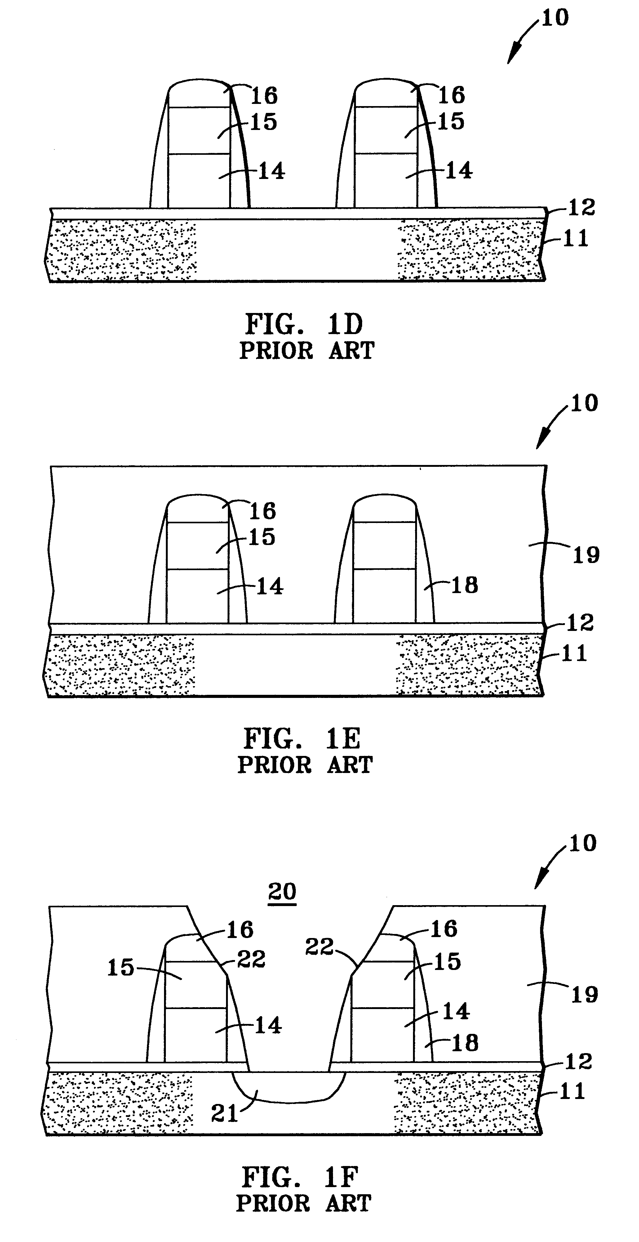
Image

Examples
Embodiment Construction
Applicant's inventor has discovered that unexpectedly relatively high level of oxygen in the above described chemistry could be profitable and significantly improve the tungsten silicide etch step by preserving the patterned Si3N4 top layer thickness and integrity. Although, the method of the present invention, such as disclosed hereinbelow, has been developed on an AME 5000 system equipped with an electrostatic chuck device in a M.times.P chamber, it can be extended to other plasma etcher tools.
The novel chemistry gives the high Si3N4 / WSix selectivity that is required to preserve the masked Si3N4 top layer thickness and integrity and the desired etch anisotropy during WSix etching, which are essential elements to produce the desired vertical profiles at the end of the GC stack fabrication process. The idea at the base of the present invention is thus to use an unusually high oxygen content in the C12 / HCl / O2 gas mixture. The novel etch chemistry has been found to drastically limit t...
PUM
 Abstract
Description
Claims
Application Information