

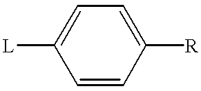
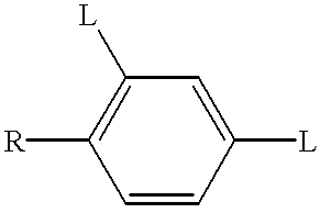
Liquid crystalline charge transport material
a charge transport material and liquid crystal technology, applied in the direction of thin material processing, corona discharge, instruments, etc., can solve the problems of lowering the charge mobility, affecting the charge transport ability and response speed of a film formed from the material, and many practical problems, so as to achieve excellent charge transport properties, reduce the effect of smectic properties of the liquid crystal
- Summary
- Abstract
- Description
- Claims
- Application Information
AI Technical Summary
Benefits of technology
Problems solved by technology
Method used
Image

Examples
example 2
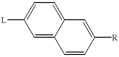
The hole and electron carrier mobility of a naphthalene compound liquid crystal (2-(4'-octylphenyl )-6-dodecyloxynaphthalene, Crystal-79 .3.degree. C.-SmX.sub.1 -100.4.degree. C.-SmX.sub.2 -121.3.degree. C.-Iso.) was measured and found to be 1.5.times.10.sup.-3 cm.sup.2 / v.s in smectic X.sub.1 phase and 2.5.times.10.sup.-4 cm.sup.2 / v.s in smectic X.sub.2 phase.
example 3
Two glass substrates each having an ITO electrode (surface electric resistance: 100-200 .OMEGA. / .quadrature.) provided by vacuum film formation were laminated onto each other so that the ITO electrodes faced each other while providing a gap therebetween using spacer particles, thereby preparing a cell. A naphthalene compound liquid crystal (2-(4'-octylphenyl)-6-dodecyloxynaphthalene) was mixed with 1% by mole of a luminescent material (3-(2-benzothiazolyl)-7-(diethylamino)-2H-1-benzopyran-2-one (manufactured by Nihon Kanko Shikiso Kenkyusho (Japan Photosensitive Dye Laboratory), oscillating wavelength: 607-585 nm), and the mixture was poured at 125.degree. C. into the cell. A d.c. electric field of 250 V was applied to the cell in a dark place. As a result, light emission derived from the fluorescent wavelength of the luminescent dye was observed.
example 4
A glass substrate having an ITO electrode (surface electric resistance: 100-200 .OMEGA. / .quadrature.) provided by vacuum film formation and a glass substrate having a silver electrode (specific resistance: not more than 1 .OMEGA. / cm, layer thickness: 3000 .ANG.) were laminated onto each other so that the electrodes faced each other while providing a gap therebetween using spacer particles, thereby preparing a cell. A naphthalene compound liquid crystal (2-(4'-octylphenyl)-6-dodecyloxynaphthalene) was mixed with 1% by mole of a luminescent material (3-(2-benzothiazolyl)-7-(diethylamino)-2H-1-benzopyran-2-one (manufactured by Nihon Kanko Shikiso Kenkyusho (Japan Photosensitive Dye Laboratory), oscillating wavelength: 607-685 nm), and the mixture was poured at 125.degree. C. into the cell. A d.c. electric field of 250 V was applied to the cell in a dark place. As a result, light emission derived from the fluorescent wavelength of the luminescent dye was observed.
PUM
| Property | Measurement | Unit |
|---|---|---|
| thickness | aaaaa | aaaaa |
| surface electric resistance | aaaaa | aaaaa |
| oscillating wavelength | aaaaa | aaaaa |
Abstract
Description
Claims
Application Information