Color organic EL display and fabrication method thereof

a technology of organic el and evaporation film, applied in diffusion transfer processes, instruments, lenses, etc., can solve the problems of deterioration of accuracy, large light emission device area, and difficulty in finely forming metal sheets corresponding to fine light emission device areas

Inactive Publication Date: 2001-09-04
SAMSUNG DISPLAY CO LTD
View PDF3 Cites 39 Cited by
  • Summary
  • Abstract
  • Description
  • Claims
  • Application Information

AI Technical Summary

Problems solved by technology

However, in such a method, it is difficult to finely form a metal sheet corresponding to a fine light emission device area and accurately form an evaporation film to a light emission device area because of bend and expansion of a metal sheet.
In addition, when the metal sheet contacts the positive hole transporting layer, the element portion breaks and thereby the light emission device becomes large and deteriorates accuracy.
Thus, the resolution of the resultant display deteriorates.
Thus, the conventional method is not sufficient for the visual recognition characteristic and fabrication yield.
In other words, it is not suitable to use the shadow mask method of which an opening portion is formed in a metal sheet.
Thus, the dopant materials contaminate the acceptor elements.
Consequently, color purity deteriorates.
Thus, the fabrication yield deteriorates.
Moreover, since the heating temperature of the sublimation materials should be precisely controlled, the heating method using a heating roller causes the materials to unevenly sublimate.

Method used


Image

  • Color organic EL display and fabrication method thereof
  • Color organic EL display and fabrication method thereof
  • Color organic EL display and fabrication method thereof

Examples


first embodiment

[First Embodiment]

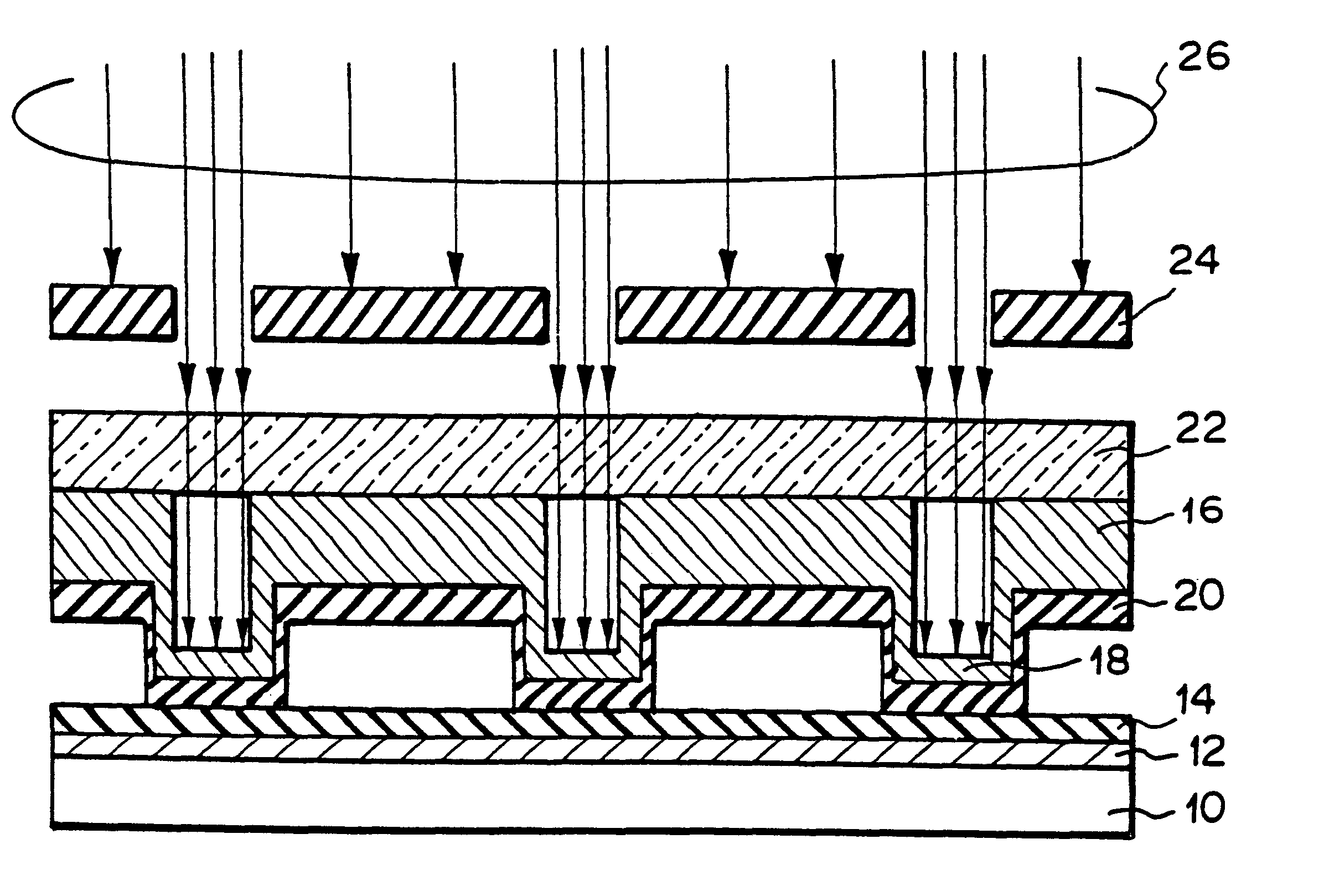
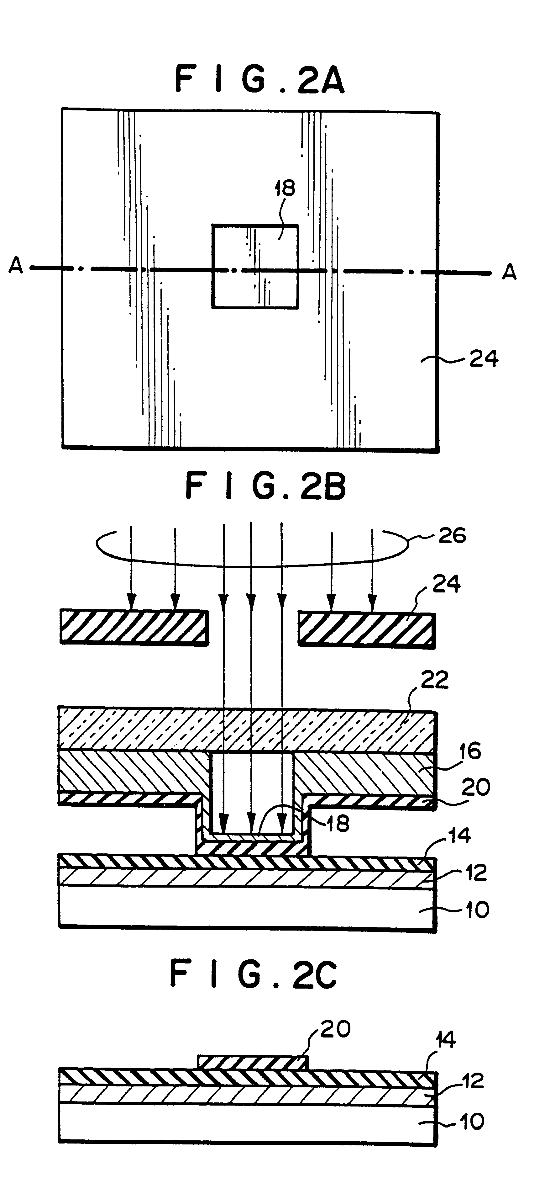
FIG. 2A is a plan view for explaining a fabrication method for a color organic EL display using a light emission organic material 20 that is sublimated and transferred according to a first embodiment of the present invention. FIG. 2B is a sectional view taken along line A--A of FIG. 2B. FIG. 2C is a sectional view showing the color organic EL display that has been fabricated according to the first embodiment of the present invention.

On a glass substrate 10 that becomes the front surface of the display, an ITO film 12 that is a transparent conductor film and a positive hole transporting layer 14 are formed. In FIG. 2B, a transfer substrate has a protrusion portion 18 disposed on a metal sheet 16. The shape of the protrusion portion 18 corresponds to the shape of a light emission device area. The height of the protrusion portion 18 is 50 .mu.m or less. The thickness of the protrusion portion 18 is around 10 .mu.m in consideration of the heat conductivity. In this sta...

second embodiment

[Second Embodiment]

Next, with reference to FIGS. 3A, 3B, and 3C, a fabrication method for a color display according to a second embodiment of the present invention will be described.

The steps until the positive hole transporting layer 14 in the second embodiment is formed are the same as those in the first embodiment.

A protrusion portion 18 of a metal sheet 16 is formed with a size of 100 .mu.m.times.100 .mu.m and with a color arrangement pitch of 300 .mu.m. The height of the protrusion portion 18 is 50 .mu.m. The inner thickness of the protrusion portion 18 is 10 .mu.m. As a red light emission organic material, alumiquinoline complex and 4-dicyanomethylene-2-methyl-6-(p-dimethylaminostyryl)-4H-pyrane (DCM, doping concentration=5 wt %) as a dopant are co-evaporated for 25 nm. As an electron conveying layer, alumiquinoline complex is evaporated for 35 nm. After a light emission element portion is aligned with the protrusion portion 18, a glass plate 22 is placed on the metal sheet 16...

third embodiment

[Third Embodiment]

Next, a third embodiment of the present invention will be described. In the third embodiment, the contrast between devices is improved.

An ITO film 12 is formed on a glass substrate 10. Thereafter, a pattern of the ITO film 12 is photo-lithographed and etched. As an insulation wall 30 whose width is 5 .mu.m and whose height is 40 .mu.m, an SiO.sub.2 film is photo-lithographed and etched.

Next, as a positive hole transporting material, N, N'-diphenyl-N, N'-di(3-methylphenyl)-1,1'-biphenyl-4,4'-diamine is vacuum-evaporated for 50 nm. A positive hole transporting layer 14 is equally formed on the ITO film 12. The size of a protrusion portion 18 of a metal sheet 16 that is a transfer substrate corresponds to the size of a light emission device area disposed on a substrate 10 through an SiO.sub.2 film. The size of the protrusion portion 18 of the metal sheet 16 is 80 .mu.m.times.80 .mu.m. The pitches of protrusion portions 18 are 30 .mu.m. The height of each protrusion po...


PUM

PropertyMeasurementUnit
heightaaaaaaaaaa
thicknessaaaaaaaaaa
thicknessaaaaaaaaaa

Abstract

A positive hole transporting layer (14) is formed on an ITO film so as to form a substrate (10). A light emission organic material (20) is formed on the front surface of a convex protrusion portion (18) of a metal sheet (16). The front surface of the positive hole transporting layer (14) and the convex protrusion portion (18) are clamped with a glass plate (22). Laser light is radiated to the interior of the convex protrusion portion (18) through a shielding plate with an opening portion whose size corresponds to the size of the convex protrusion portion (18). The light emission organic material formed on the front surface of the convex protrusion portion (18) sublimates and transfers to the positive hole transporting layer (14). These steps are performed for areas of three color light emission devices.

Description

1. Field of the InventionThe present invention relates to a color organic EL display using electroluminescence of an organic compound material and to a fabrication method thereof.2. Description of the Related ArtIn a conventional organic electroluminescence display apparatus using a color organic EL display, it is important to selectively form color light emission organic materials as color light emission devices in a fine pattern on a transparent electrode.In providing such color emission devices on a transparent electrode a shadow mask method has been used in which, when a light emission organic material is selectively evaporated and formed as layer, an opening portion of a shadow mask is formed in a metal sheet (see FIG. 1). In FIG. 1, a transparent anode 102 is disposed below a transparent glass substrate 101. An organic fluorescent film and an organic positive hole transporting layer 103 are disposed below the anode 102. A metal cathode 106 that is selectively evaporated is dis...

Claims


Application Information

Patent Timeline
Patent Type & Authority Patents(United States)
IPC IPC(8): H01L27/28H01L27/32H01L51/05H01L51/30G02B3/00B44C1/17H01L51/00H01L51/50H05B33/10H05B33/12H05B33/14
CPCH01L27/3211H01L51/0013H01L51/0081H01L51/0051H10K59/35H10K71/18H10K85/611H10K85/324H05B33/14
Inventor FUKUZAWA, SHINICHIOTSUKI, SHIGEYOSHI
Owner SAMSUNG DISPLAY CO LTD
Why Eureka
Try Eureka