Method and device for high-temperature, high-pressure treatment of semiconductor wafer

Inactive Publication Date: 2001-09-04
KOBE STEEL LTD
View PDF8 Cites 28 Cited by
  • Summary
  • Abstract
  • Description
  • Claims
  • Application Information

AI Technical Summary

Problems solved by technology

The most different point of the heating treatment of the semiconductor substrate from the treatment of other materials and members is that adhesion of dust called particles cannot be permitted.
The second different point is that extremely high productivity, or a short-time treatment is required because of the treatment within a clean room having high construction and maintenance costs.
Another problem in such a prior art is that the rise of internal temperature of the bell jar is rather delayed to makes the precise program control of temperature to time, in contrast with the quick temperature rise of the heater part when a high-speed temperature rise is performed in temperature rising process, because the wafers as workpiece are surrounded by the bell jar and heated by the heater arranged on the outside thereof.
In cooling process, also, the bell jar is the barrier to diffusion of heat to cause the problem of requiring much time for cooling.
In addition to the situation of the prior art as described above, the recent tendency of enlargement of the wafer or change in diamete

Method used


Image

  • Method and device for high-temperature, high-pressure treatment of semiconductor wafer
  • Method and device for high-temperature, high-pressure treatment of semiconductor wafer
  • Method and device for high-temperature, high-pressure treatment of semiconductor wafer

Examples


Embodiment Construction

A preferred embodiment of this invention is further illustrated on the basis of the accompanying drawings.

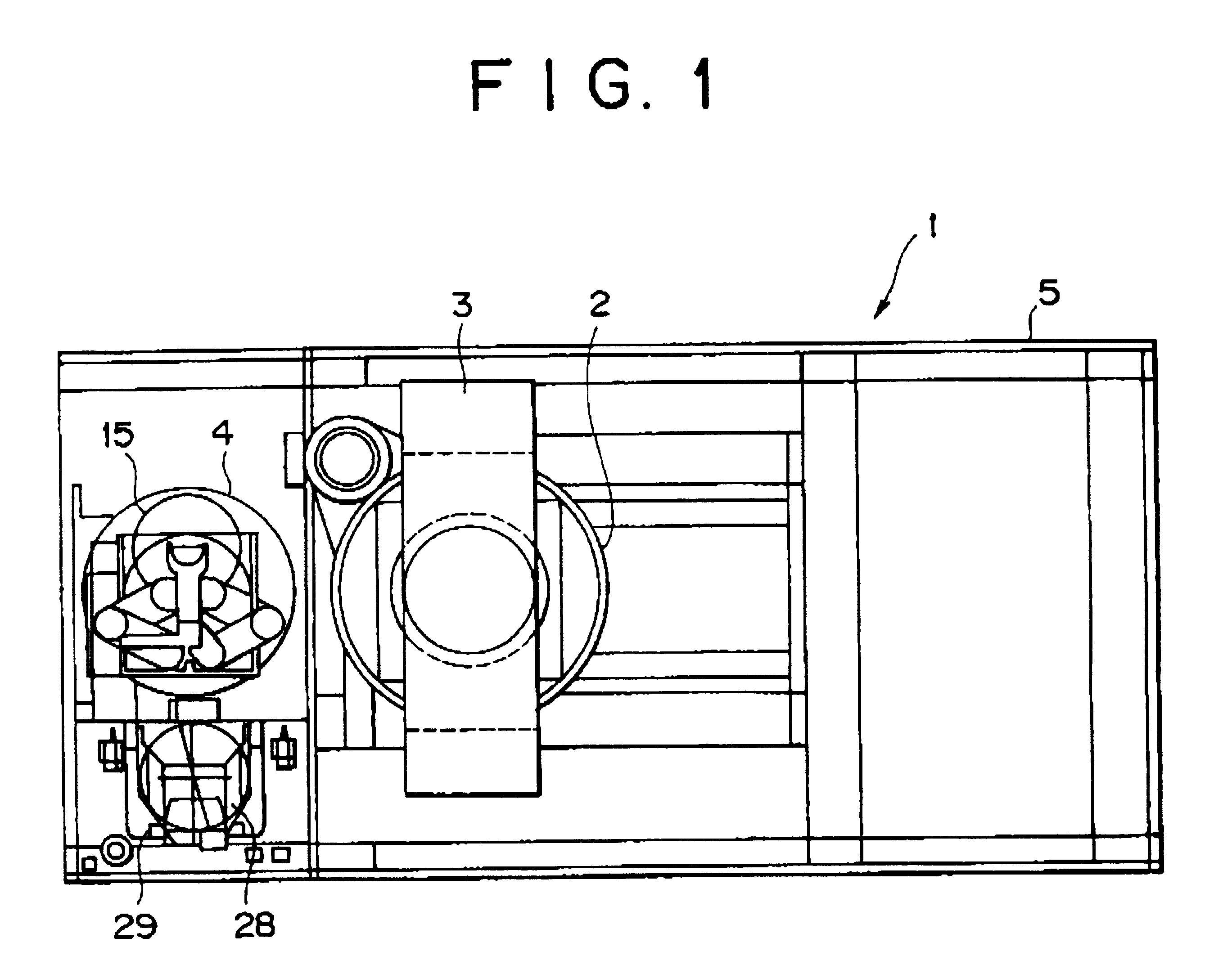
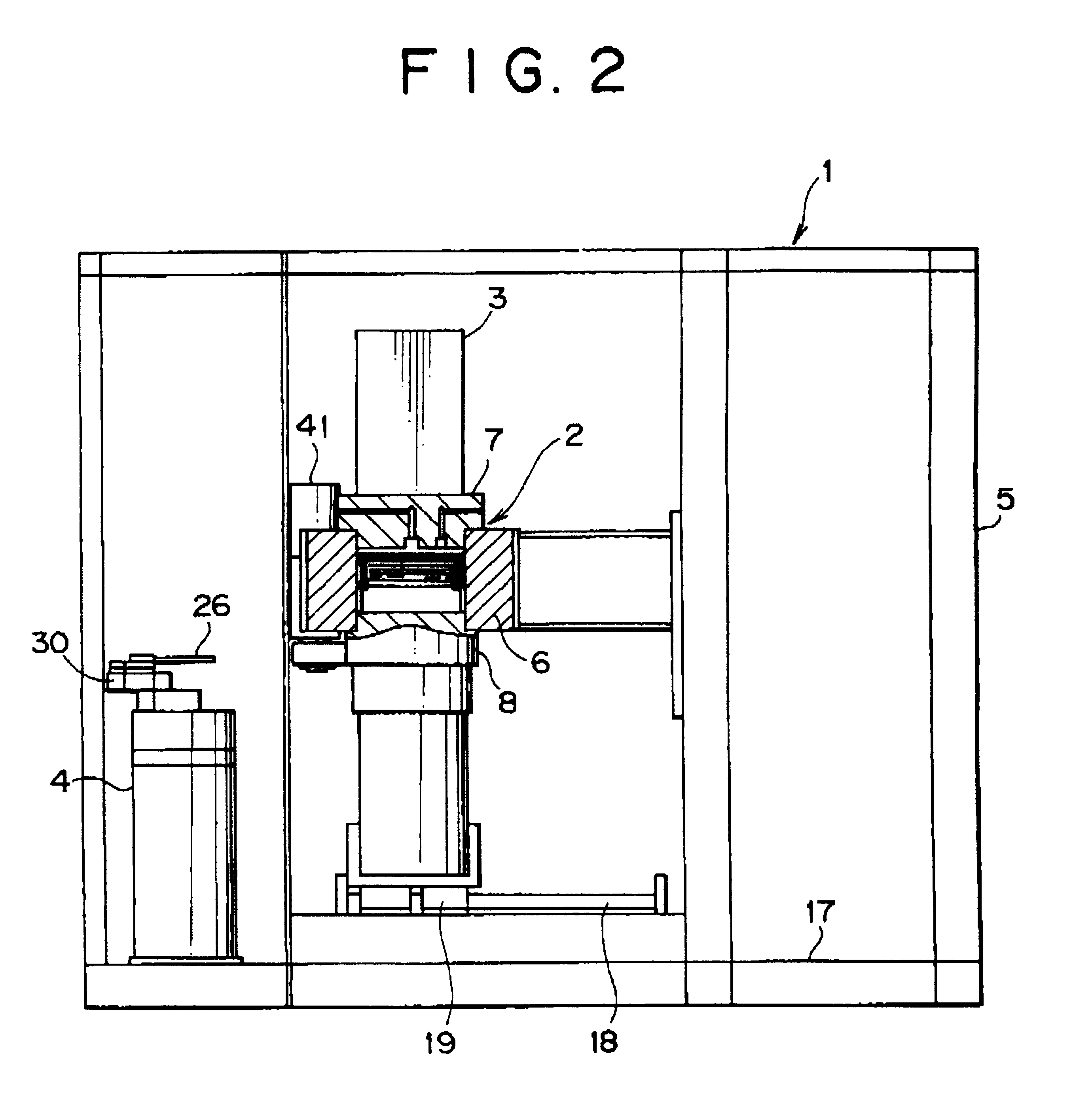
FIGS. 1 and 2 are an example of the body part of a semiconductor high-temperature, high-pressure treatment device 1 according to this invention, which particularly shows the operating state at a high pressure with a high-pressure gas charged in a high-pressure vessel (pressure vessel) 2.

The body part is formed of the high-pressure vessel 2 including a press frame 3, a wafer transfer robot (transfer means) 4, and a casing 5 for housing the whole of them.

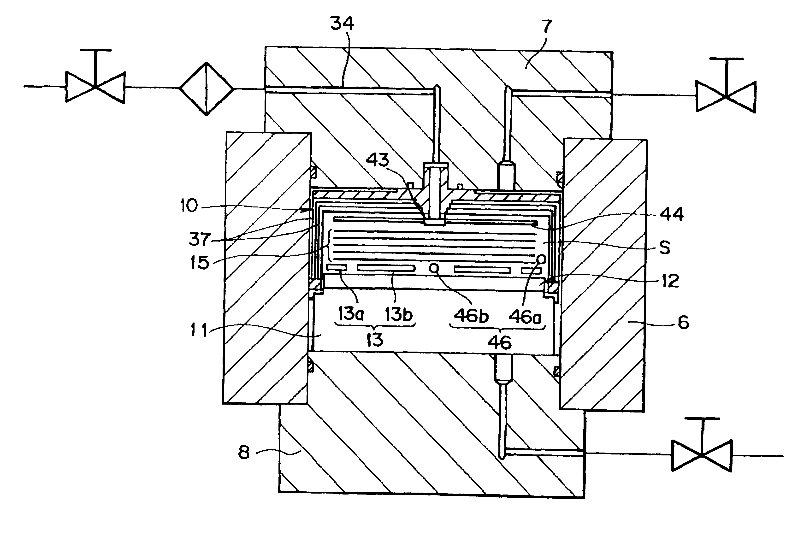
As shown in FIG. 3, the high-pressure vessel 2 is formed of a high-pressure cylinder 6, an upper lid 7, a lower lid 8, and the press frame 3 for supporting the axial load acting on the upper and lower lid 7, 8. A heat insulating structure 10 is integrated into the space S formed by the upper lid 7 and the cylindrical part 6, and a heater 13 divided into two radially inner and outer zones (heater elements 13a, 13b) is arranged on a...


PUM

PropertyMeasurementUnit
Temperatureaaaaaaaaaa
Pressureaaaaaaaaaa
Poweraaaaaaaaaa

Abstract

In a high-temperature, high-pressure treatment method for semiconductor wafer for charging a wafer-like semiconductor material in a pressure vessel, forcing and pressurizing an inert gas such as argon thereto, and raising the temperature by heating by use of an electric resistance type heater, wafers are vertically stacked in the treatment chamber, and the heater is arranged within the treatment chamber to perform the treatment while supplying a heating power by DC to the heater, whereby generation of particles from the heater is suppressed.

Description

1. Field of the InventionThis invention relates to a method and device for treating ULSI semiconductors represented by Si wafer under high-temperature, high-pressure atmosphere and, particularly, to a method and device for treating semiconductor wafers in a small lot of 1 to 25 pieces.This invention further relates to a device used for a treatment of removing pores mainly by the pressure of an inert gas, such as a so-called pressure filling method for wiring film (high-pressure reflow process) of pressure treating a wafer having a copper alloy wiring film formed thereon by PVD, electrodeposition, CVD or the like by the inert gas pressure, and a method for using it, wherein the heating is performed in a short time to reduce generation of particles causing the contamination of a semiconductor substrate.2. Description of the Related ArtAs the process of treating semiconductor wafers under a high-pressure gas atmosphere by use of a vertical boat (wafer stacking jig), high-pressure oxida...

Claims


Application Information

Patent Timeline
IPC IPC(8): H01L21/00H01L21/70H01L21/768H01L21/3205F27D11/02
CPCH01L21/76882H01L21/67109H01L21/67103H01L21/67248
Inventor FUJIKAWA, TAKAONARUKAWA, YUTAKAMASUDA, TSUNEHARUKADOGUCHI, MAKOTO
Owner KOBE STEEL LTD
Why Eureka
Try Eureka