Electrolytic deposition of dielectric precursor materials for use in in-laid gate MOS transistors

a technology of dielectric precursor materials and inlaid gate mos, which is applied in the direction of basic electric elements, electrical equipment, and semiconductor devices, etc., can solve the problems of reducing performance by about 15% or more, adversely affecting polysilicon gates, and increasing the effective gate oxide thickness ("eot")

Inactive Publication Date: 2001-10-09
GLOBALFOUNDRIES US INC
View PDF9 Cites 103 Cited by
  • Summary
  • Abstract
  • Description
  • Claims
  • Application Information

AI Technical Summary

Problems solved by technology

However, polysilicon-based gate electrodes incur a number of disadvantages, including, inter alia: (1) as device design rules decrease to below about 0.20 .mu.m, polysilicon gates are adversely affected by poly depletion, wherein the effective gate oxide thickness ("EOT") is increased.
Such increase in EOT can reduce performance by about 15% or more; (2) polysilicon-based gate electrodes have higher resistivities than most metal or metallic materials and thus devices including polysilicon as electrode or circuit materials operate at a much slower speed than equivalent devices utilizing metalbased materials.
Further, a significant portion of the voltage applied to the gate during operation is dropped in the polysilicon due to the poor conductivity of silicon.
The use of metal or metallic materials as replacements for polysilicon-based materials as gate electrodes in MOS and/or CMOS devices incurs several difficulties, however, which difficulties must be considered and overcome in any metal-based gate electrode process scheme, including: (1) metal and/or metal-based gates cannot withstand the higher temperatures and oxidative ambients which conventional polysilicon-based gate electrode materials can withstand; (2) several candidate metals or metallic materials for use as gate electrodes do not exhibit adequate adhesion in film form to surrounding layers of different materials when these metals or metallic materials are patterned to very small geometries; (3) some metal or metallic films are difficult to lithographica...

Method used


Image

  • Electrolytic deposition of dielectric precursor materials for use in in-laid gate MOS transistors
  • Electrolytic deposition of dielectric precursor materials for use in in-laid gate MOS transistors
  • Electrolytic deposition of dielectric precursor materials for use in in-laid gate MOS transistors

Examples


Embodiment Construction

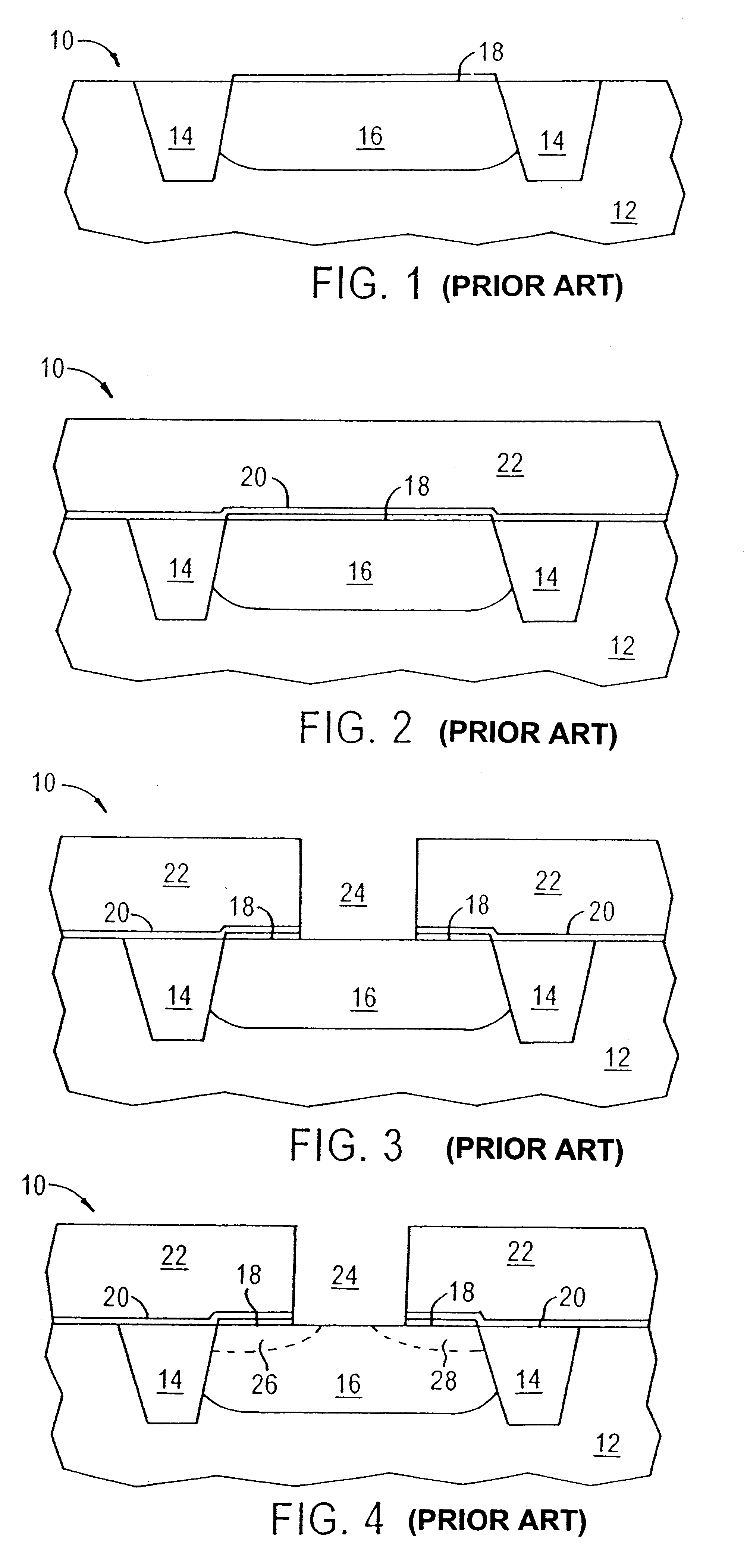
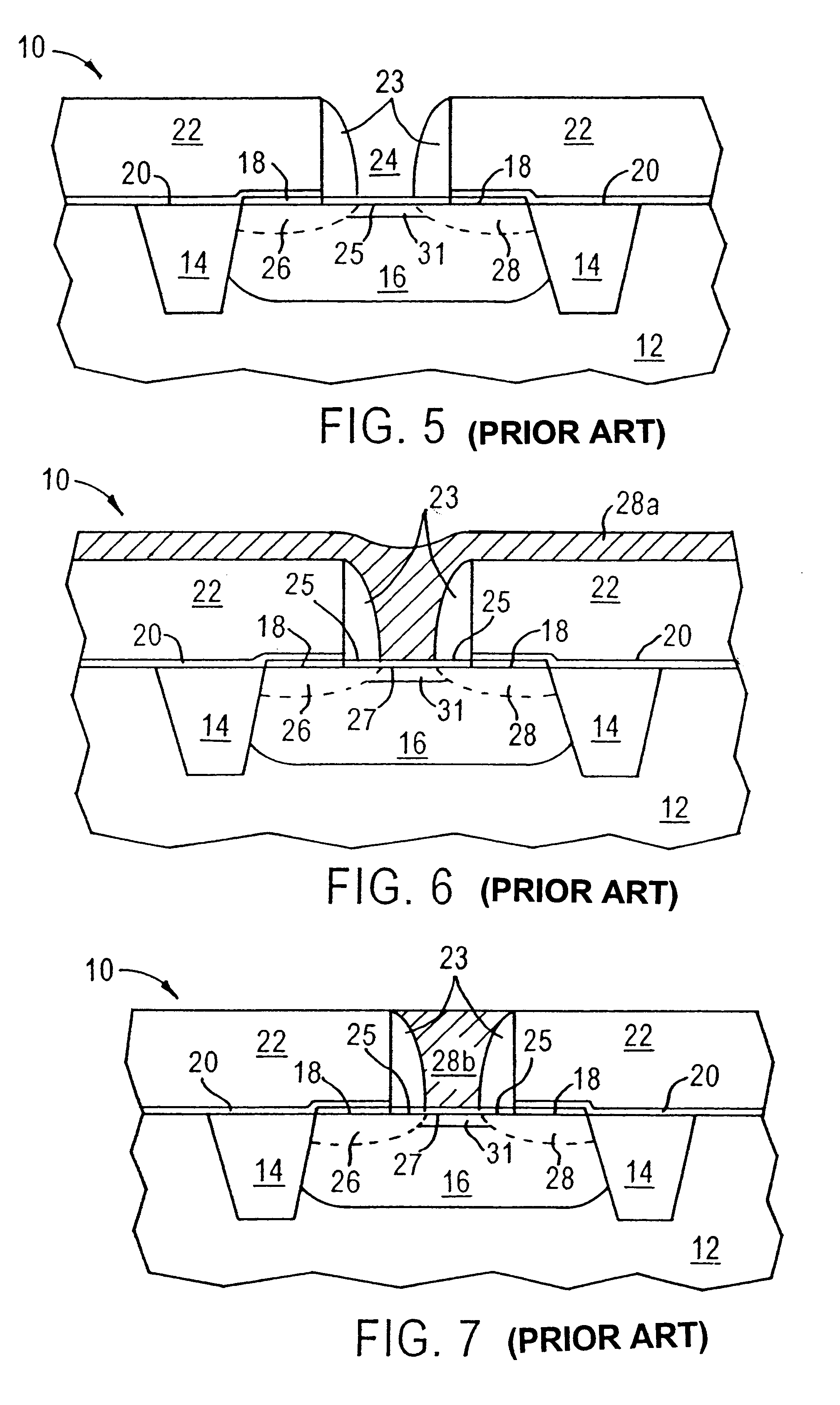
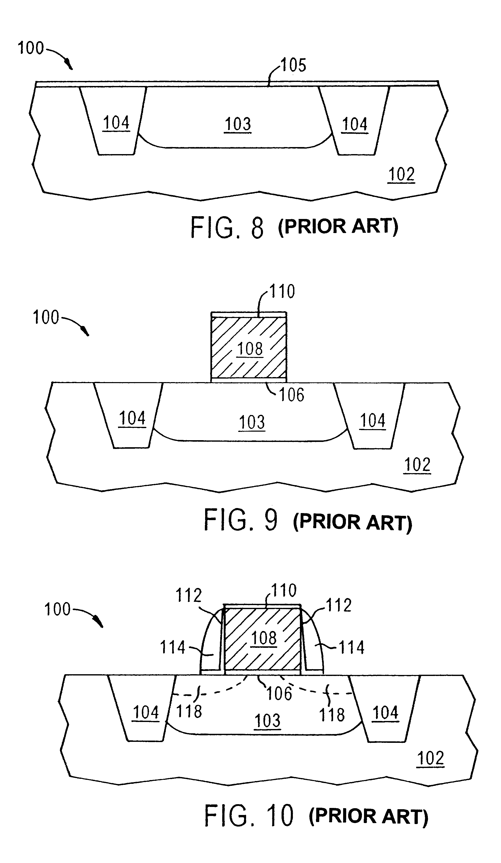
The present invention is based upon the discovery that formation of high quality dielectric layers, i.e., illustratively but not limited to, high-k dielectric layers comprised of at least one refractory metal oxide or silicate, for use as gate insulator layers in in-laid gate (e.g., in-laid metal gate) MOS transistors and CMOS devices, can be readily formed by a process which prevents, or at least substantially reduces, access or exposure of the semiconductor (typically of Si but not limited thereto) substrate surface to oxygen at least during the initial stage(s) of the process. A key feature of the present invention is the formation on the semiconductor substrate surface, by relatively low temperature electrolytic deposition, e.g., cathodic electroplating, of a thin layer of metal or metalcontaining dielectric precursor material, e.g., a refractory metal layer such as of zirconium and / or hafnium or a lanthanum series transition metal, which layer of precursor material is subsequen...


PUM


Abstract

High quality dielectric layers, e.g., high-k dielectric layers comprised of at least one refractory or lanthanum series transition metal oxide or silicate, for use as gate insulator layers in in-laid metal gate MOS transistors and CMOS devices, are formed by electrolytically plating a metal or metal-based dielectric precursor layer comprising at least one refractory or lanthanum series transition metal, on a semiconductor substrate, typically a silicon-based substrate, and then reacting the precursor layer with oxygen or with oxygen and the semiconductor substrate to form the at least one refractory or lanthanum series transition metal oxide or silicate. The inventive methodology prevents, or at least substantially reduces, oxygen access to the substrate surface during at least the initial stage(s) of formation of the gate insulator layer, thereby minimizing deleterious formation of oxygen-induced surface states at the semiconductor substrate/gate insulator interface.

Description

The present invention relates to methods of manufacturing a semiconductor device, e.g., an MOS transistor device, wherein the source, drain, channel regions, and the gate electrode of the transistor are formed in a self-aligned manner utilizing an in-laid ("damascene") gate and corresponding processing techniques therefor. The present invention has particular utility in the manufacture of high integration density semiconductor devices employing design rules of 0.20 .mu.m and below, e.g., 0.15 .mu.m and below.BACKGROUND OF THE INVENTION AND RELATED ARTThe escalating requirements for high density and performance (e.g., transistor and circuit speeds) associated with ultra-large scale integration ("ULSI") devices necessitate design rules for component features of 0.20 .mu.m and below, such as 0.15 .mu.m and below, such as source, drain, and gate regions and electrodes therefor formed in or on a common semiconductor substrate, challenges the limitations of conventional materials and manu...

Claims


Application Information

Patent Timeline
IPC IPC(8): H01L21/02H01L21/336H01L29/51H01L21/28H01L21/316H01L29/40
CPCH01L21/28194H01L21/31683H01L29/517H01L29/66583H01L21/02244H01L21/02258
Inventor BUYNOSKI, MATTHEW S.BESSER, PAUL R.XANG, QIKING, PAUL L.PATON, ERIC N.
Owner GLOBALFOUNDRIES US INC
Why Eureka
Try Eureka