Self-waveguide optical circuit

a self-waveguide, optical circuit technology, applied in the direction of optical waveguide light guide, instruments, nanotechnology, etc., can solve the problems of large volume, large size of collimator itself, and severe conditions to an accuracy

Inactive Publication Date: 2001-11-13
NEC CORP
View PDF5 Cites 73 Cited by
  • Summary
  • Abstract
  • Description
  • Claims
  • Application Information

AI Technical Summary

Problems solved by technology

However, the conventional free space propagation optical circuits and waveguide optical circuits have the following problems.
The free space propagation optical circuits have problems in connection with a collimator.
A first problem is that severe conditions are imposed to an accuracy of determining a position of an optical point source or a pinhole, that is, to a divergent angle of an incident ray.
A second problem is that the collimator itself is large and requires a large volume for mounting.
As a result, a subsidiary problem arises that a spot size of an exit ray becomes larger than the size of the optical source or the pinhole.
In the waveguide optical circuits, waveguides are difficult to be crooked at a steep angle.
Since a curvature radius in the order of centimeter is necessary under the present circumstances, the whole circuit inevitably has the order of centimeter and miniaturization is difficult.
Since the total reflection conditions are employed as a principle of guiding rays as mentioned earlier, a steep crook invites a large radiation loss.
Although formation of a complete crystal having a wavelength band in which no propagation of rays occurs and introduction of a linear defective structure are required in the self-waveguide optical circuit employing the photonic crystals, realization of the complete crystal is technically difficult under the present circumstances.
It is extremely difficult to intentionally introduce the defective structure into the complete crystal for forming linear or crooked waveguides.
For example, in order to constitute such a linear or crooked waveguide structure in a wavelength band of rays around 1.5 micronmeters employed for current optical communications, control of processing in the order of at least 0.1 micronmeter and a high aspect ratio are required, and these are extremely difficult under the present circumstances of techniques.
However, absorption is generally increased due to a resonance effect in a wavelength band having a large non-linearity, and a phenomenon in which the strength of rays is attenuated along the propagation direction is difficult to be avoided.
In this case the strength of rays must be sufficiently high which reaches to an unrealistic value (watt-level) in an optical circuit having a purpose of information processing or optical connection of a short distance.
Attainment of miniaturization, high integration and high speed operation is difficult in all of the conventional optical circuits, and accordingly elevation of a transmission efficiency is also difficult.

Method used


Image

  • Self-waveguide optical circuit
  • Self-waveguide optical circuit
  • Self-waveguide optical circuit

Examples


embodiment 1

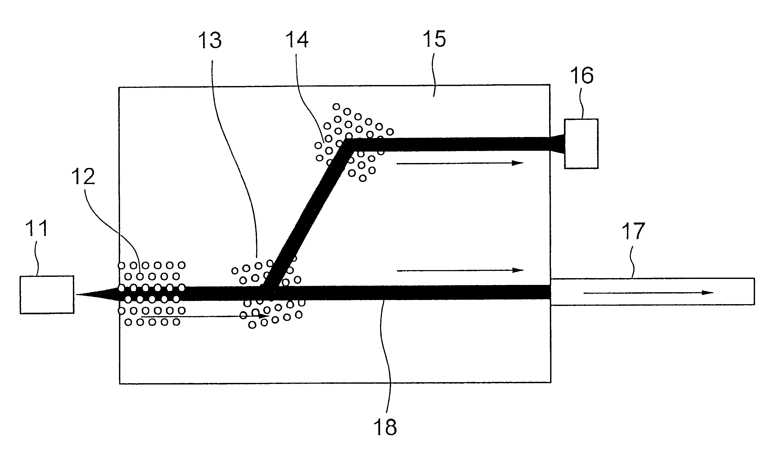
As shown in FIG. 7, a self-waveguide optical circuit of the present invention is formed by an optical circuit substrate 15, a razor 11 and a receptor element 16 connected to the both edges of the optical circuit substrate 15, and an optical fiber 17. In the optical circuit substrate 15, a first photonic crystal 12, a second photonic crystal 13 and a third photonic crystal 14 are partially formed.

As described later, rays propagate from the razor 11 to the optical fiber 17 and to the receptor element 16 through the photonic crystals 12, 13 and 14. Part of the rays diverge at the photonic crystal 13 to enter into the optical fiber 17.

The photonic crystals 12, 13 and 14 may be the same as that shown in FIGS. 3A and 3B, and have the composition and the structure already mentioned. An SiO.sub.2 buffer is positioned on an Si substrate, and SiO.sub.2 layers and amorphous Si (a-Si) layers both having the shapes reflecting the concave-convex of the triangular lattice of the SiO.sub.2 buffer a...

embodiment 2

A self-waveguide optical circuit of a second embodiment shown in FIG. 8 has an optical circuit substrate 23 forming a photonic crystal 22 on the whole surface, an incident ray side-optical fiber 21 and exit side-optical fibers 24. The structure of the photonic crystal 22 may be the same as that shown in FIGS. 3A, 3B and 3C. However, the direction of the photonic crystal 22 is selected to have the condition of "a" in FIG. 4A.

Then, the operation of the self-waveguide optical circuit of Embodiment 2 will be described referring to FIG. 8.

The exit rays from the incident ray side-optical fiber 21 are incident on the photonic crystal 22. The rays spreading in fan-shape as shown in FIG. 6A because the crystal direction is selected to have the direction "a" shown in FIG. 4A.

The propagation rays spreading in fan-shape as shown at 25 are separately incident on a plurality of the exit side-optical fibers 24 disposed on the opposite side. The exit rays from the photonic crystal advantageously ha...


PUM


Abstract

Disclosed herein is a self-waveguide optical circuit for forming optical paths by propagating rays or electromagnetic waves comprising: photonic crystals having a dielectric constant periodic structure or a dielectric constant semi-periodic structure having a period substantially corresponding to a wavelength of propagation rays, and optical paths formed by establishing a crystal direction of the photonic crystal to level the dispersion surface of the photonic crystal for obtaining a bundle of parallel rays. In accordance with the present invention, elevation of characteristics such as miniaturization, high integration, high speed operation and transmission efficiency can be obtained because a bundle of parallel rays can be obtained without forming crooked parts having an excessive curvature radius.

Description

(a) Field of the InventionThe present invention relates to a self-waveguide optical circuit, more in detail to the self-waveguide optical circuit which may easily implement miniaturization, high integration and high speed operation, has an excellent transmission efficiency, and is suitably employed in technical fields such as optical communication, optical control and optical information processing.(b) Description of the Related ArtConventional optical circuits can be largely divided into free space propagation optical circuits and waveguide optical circuits.The free space propagation optical circuit defines optical paths by combining individual optical components such as a collimator, a lens and a reflection mirror without formation of waveguides.As the collimator for obtaining a bundle of parallel rays among the above optical components, a lens or a concave mirror is employed. A slit or a pinhole formed on the focus of the lens or the concave mirror is precisely adjusted to obtain...

Claims


Application Information

Patent Timeline
Patent Type & Authority Patents(United States)
IPC IPC(8): G02B6/122G02B6/12
CPCB82Y20/00G02B6/1225
Inventor KOSAKA, HIDEOKAWAKAMI, SHOJIRO
Owner NEC CORP
Why Eureka
Try Eureka