Microwave and millimeter wave circuit apparatus

a circuit apparatus and micro-wave technology, applied in waveguide devices, substantially flat resonant elements, resonance antennas, etc., can solve the problems of difficult connection with a low loss, inability to measure microwave and millimeter wave characteristics using probe apparatuses or the like, etc., to achieve the effect of reducing the entire size, improving productivity and easy production

Inactive Publication Date: 2001-11-20
NEC CORP
View PDF2 Cites 139 Cited by
  • Summary
  • Abstract
  • Description
  • Claims
  • Application Information

AI Technical Summary

Benefits of technology

It is therefore an object of the present invention to provide a microwave and millimeter wave circuit apparatus which can easily be produced and is capable of reducing the entire size and improving productivity.

Problems solved by technology

Especially in the millimeter wave circuit, there is a problem that because of parasitic elements such as inductance caused by the wire bonding 74, it is difficult to perform connections with a low loss and to assure performance repeatability.
Moreover, in the conventional microwave and millimeter wave circuit apparatus shown in FIG. 8, there is a problem that it is necessary to accurately position the MMIC substrate 81 and the antenna substrate 82, complicating the assembling process.
Furthermore, since circuit elements are provided on the upper and the lower surface of the apparatus, there is a problem that when mounted on a stage it is impossible to measure microwave and millimeter wave characteristics using a probe apparatus or the like.

Method used


Image

  • Microwave and millimeter wave circuit apparatus
  • Microwave and millimeter wave circuit apparatus
  • Microwave and millimeter wave circuit apparatus

Examples


first embodiment

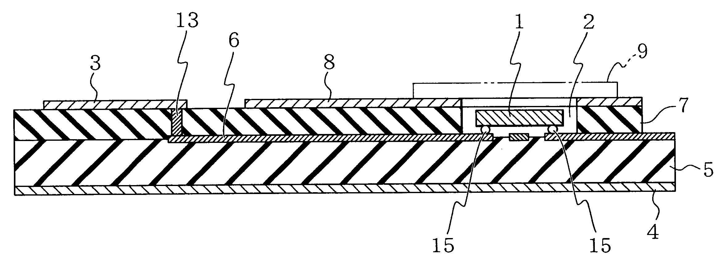
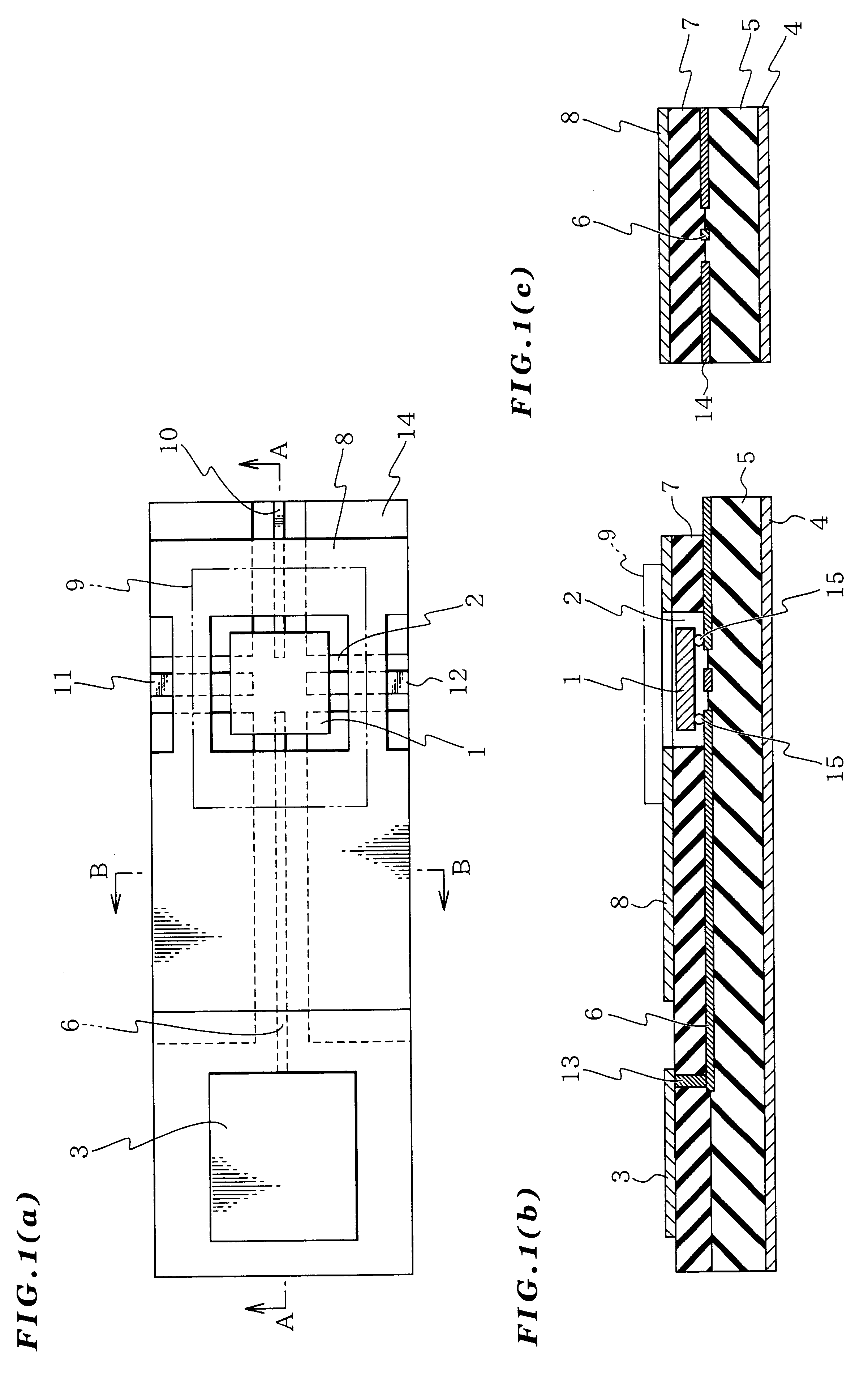
Description will now be directed to a specific microwave and millimeter wave circuit apparatus including as communication modules, for example, an MMIC having a low noise amplifier as a receiver module and a down converter for converting a signal frequency to an intermediate frequency (IF), and an antenna which are formed as an integration block, with reference to the attached drawing. FIG. 1 shows a configuration of a microwave and millimeter wave circuit apparatus according to the present invention. FIG. 1(A) is a plan view, FIG. 1(B) is a cross sectional view about the line A--A in FIG. 1(A), and FIG. 1(C) is a cross sectional view about the line B--B in FIG. 1(A).

As shown in FIG. 1(A) to FIG. 1(C), in the microwave and millimeter wave circuit apparatus according to the first embodiment, a first dielectric layer 5 is provided on a grounding metal cover 4, and a signal line 6 and a grounding metal cover 14 grounded are selectively formed on the first dielectric layer 5. Furthermor...

second embodiment

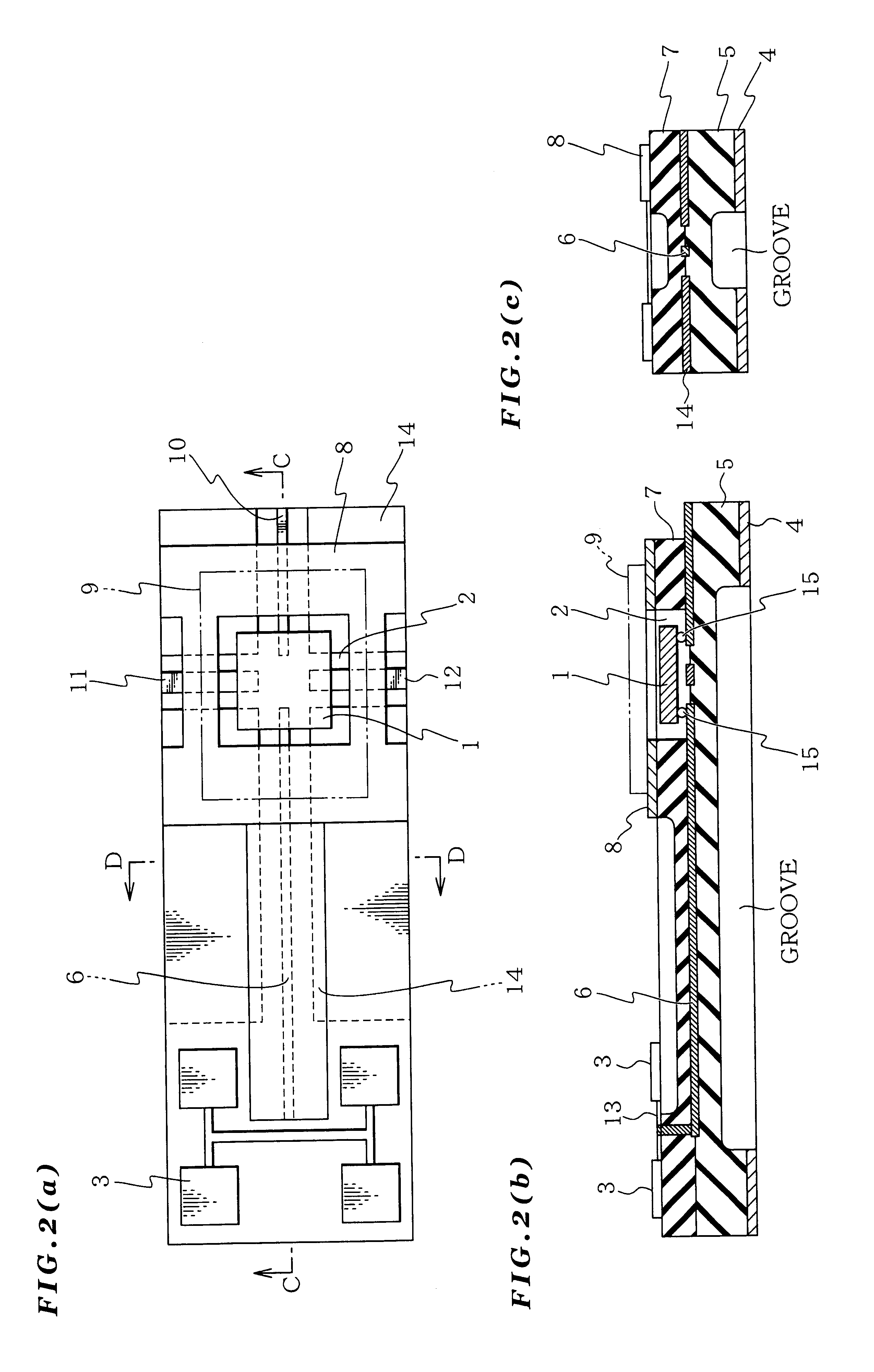
In the second embodiment, as shown in FIG. 2(A) to FIG. 2(C), no grounding metal cover is provided below the signal line 6, and the first dielectric layer 5 has a small thickness. Moreover, in the connection portion between the cavity 2 and the antenna 3, the second dielectric layer 7 has a small thickness.

In the second embodiment having the aforementioned configuration, the grounding metal cover 14 of the coplanar line of the signal line 6 and the lower most layer of the grounding metal cover 4 are in a parallel plate state, which cause generation of radiation mode as well as generation of radiation mode due to the surface wave propagation. Thus, it is possible to reduce the loss of the signal line 6 because no grounding metal cover is provided below the signal line 6. Here, by making the thickness t.sub.1 of the first dielectric layer smaller than the value obtained from the Equation 1 given below, it is possible to completely suppress the radiation mode due to the surface wave pr...


PUM


Abstract

The present invention provides a microwave and millimeter wave circuit apparatus having a reduced size and which can be produced easily, improving productivity. The microwave and millimeter wave circuit apparatus includes: a grounding conductive layer 4 grounded; a first dielectric layer 5 formed on this grounding conductive layer 4; a signal line selectively formed on this first dielectric layer 5; a second dielectric layer 7 covering at least a portion of the signal line 6; a cavity 2 formed in this second dielectric layer 7 and extending to the signal line 6; a monolithic microwave integrated circuit 1 arranged in the cavity 2 and connected to the signal line 6; and an antenna connected to the signal line 6.

Description

BACKGROUND OF THE INVENTION1. Field of the InventionThe present invention relates to a microwave and millimeter wave circuit apparatus used as a high-frequency module for a communication apparatus, radar, or the like and in more particular, to a microwave and millimeter wave circuit apparatus capable of reducing a transmission loss.2. Description of the Related ArtIn order to reduce the size of the microwave and millimeter wave circuit apparatus and perform mass production thereof, it is effective to prepare transmitter and receiver circuits of the microwave and millimeter wave as a multi-chip module (MCM) and make this transmitter and receiver circuits, which is the multi-chip module, as an integration block with an antenna. FIG. 7 schematically shows a microwave and millimeter wave circuit apparatus conventionally suggested as an integration module having an antenna.In this conventional microwave and millimeter wave circuit apparatus, a metal case package 71 contains a monolithic ...

Claims


Application Information

Patent Timeline
Patent Type & Authority Patents(United States)
IPC IPC(8): H01Q23/00H01Q9/04H01Q1/38H01P5/10H01P5/08H01Q13/08H01Q13/10
CPCH01Q1/38H01Q9/0407H01Q23/00H01L2224/16H01L2224/48137H01L2924/13062H01L2224/16225H01L2224/16227H01L2224/4823H01L2924/01079H01L2924/09701H01L2924/14H01L2924/1423H01L2924/15153H01L2924/1517H01L2924/16152H01L2924/19041H01L2924/30107H01L2224/48091H01L2924/01019H01L2924/00014H01L2924/00H01L2223/6677
Inventor OHATA, KEIICHIMARUHASHI, KENICHIITO, MASAHARU
Owner NEC CORP
Why Eureka
Try Eureka