
Method of producing semiconductor device

a semiconductor and device technology, applied in the direction of semiconductor/solid-state device details, coatings, solid-state devices, etc., can solve the problem of lower reduction capability of h.sub.2, and achieve the effect of improving the conformality of the ti film formed and improving the reliability of the contact par

Inactive Publication Date: 2001-12-18
SONY CORP
View PDF6 Cites 17 Cited by
  • Summary
  • Abstract
  • Description
  • Claims
  • Application Information

AI Technical Summary

Benefits of technology

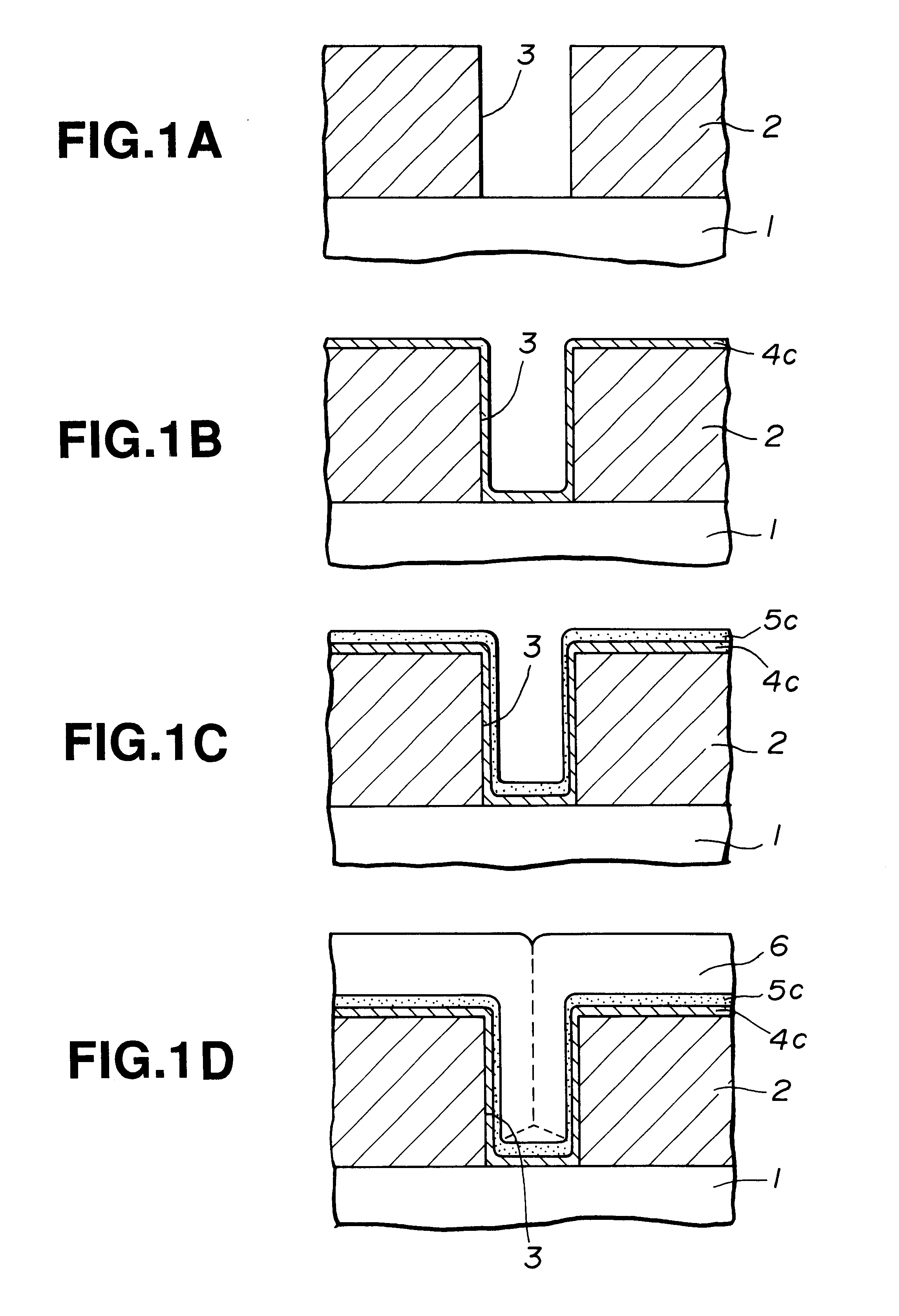
It is an object of the present invention to provide a method for producing a semiconductor device which is adapted for improving conformality of the Ti film formed by the ECR plasma CVD method and for improving reliability of the contact part.
The group IVB element includes three types, of elements that is, Ti, zirconium (Zr) and hafnium (Hf). Forming the Ti film using a TiCl.sub.4 gas is particularly effective.
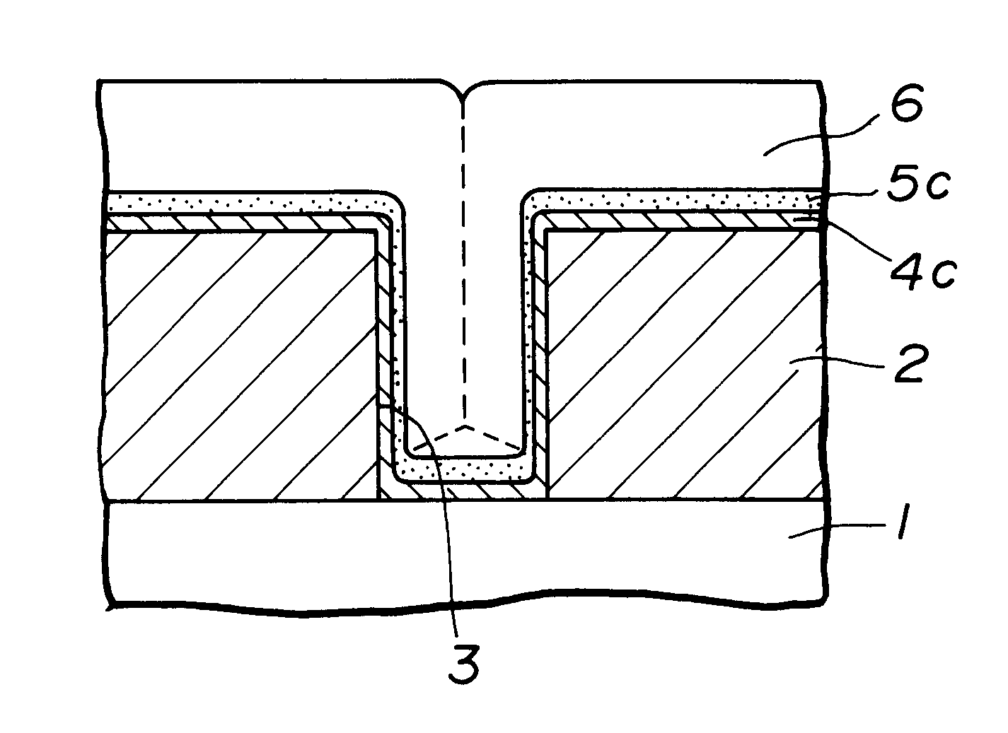
As the Ti film is thus formed conformally, even when a TiN film is stacked on the Ti film by the CVD method, a film inheriting the property of the underlying film can be grown. Thus, a risk of generating a crack in the corner part of the contact hole is eliminated.

Problems solved by technology

Although the upper limit of the flow ratio is not particularly defined, an excessively large flow ratio may lower the reduction capability of H.sub.2, disturbing achievement of practical film forming speed.

Method used


Image

  • Method of producing semiconductor device
  • Method of producing semiconductor device
  • Method of producing semiconductor device

Examples


example 2

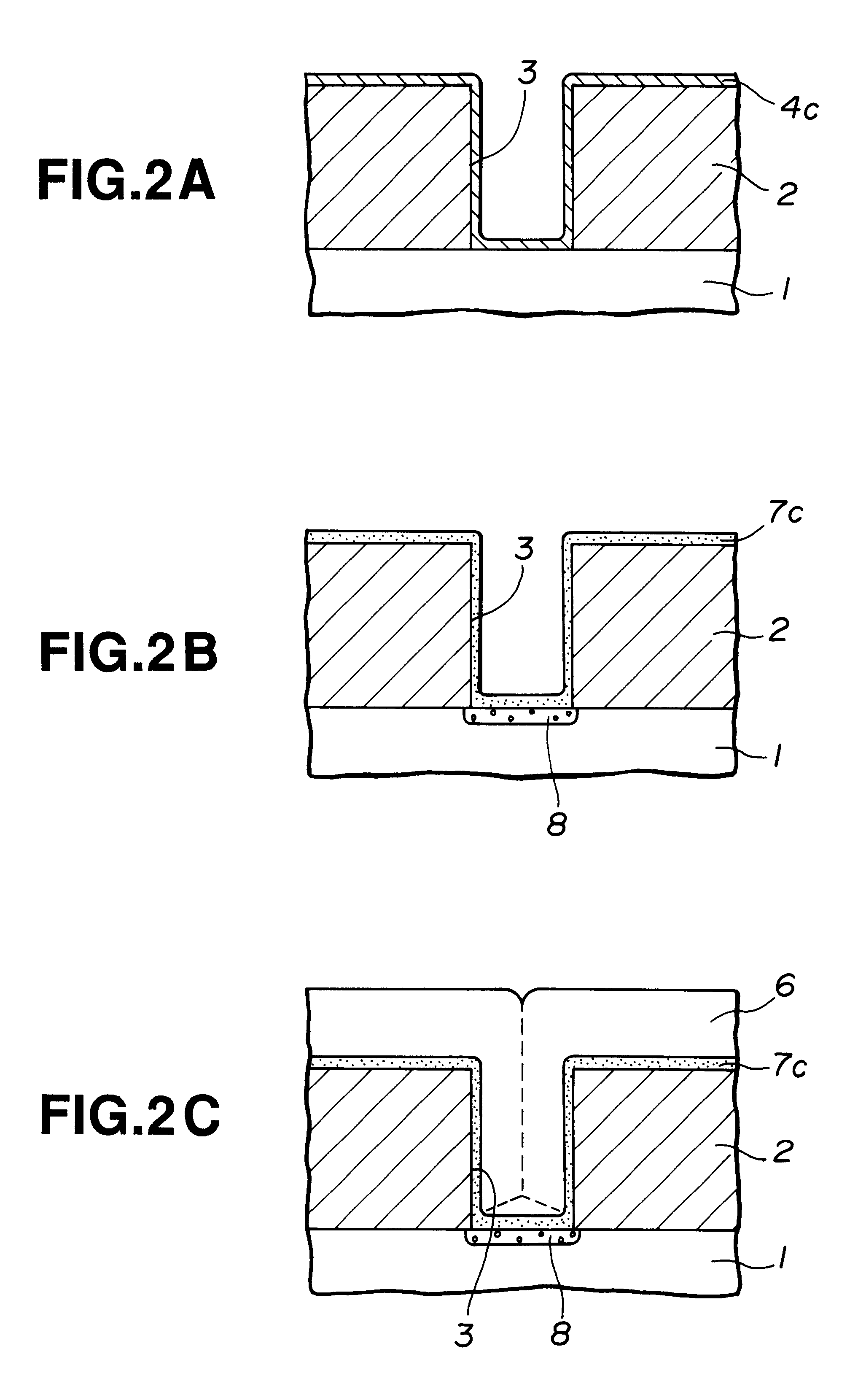
In the present example, a Ti film was conformally formed, and then the Ti film was annealed in a nitrogen-containing atmosphere to form a TiN film in a self-aligned manner. This process will be described with reference to FIGS. 2A to 2C. Reference numerals of FIGS. 2A to 2C are partly the same as those of FIGS. 1A to 1D.

First, a wafer as shown in FIG. 2A, having a Ti film 4c formed thereon in a manner similar to Example 1, was set on an annealing device and was nitrided at annealing temperatures of 500 to 900.degree. C. for an annealing time of 30 to 120 seconds in an N.sub.2 atmosphere or an ammonium (NH.sub.3) atmosphere.

By this nitriding anneal, the Ti film 4c was changed into a TiN film 7c on an SiO.sub.2 interlayer insulating film 2, as shown in FIG. 2B.

A major part of the Ti film 4c was changed into the TiN film 7c on the bottom of the contact hole 3, and a titanium / silicide (TiSi.sub.2) layer 8 was formed in a self-aligned manner on the boundary face with the Si substrate 1. ...


PUM

PropertyMeasurementUnit
thicknessaaaaaaaaaa
diameteraaaaaaaaaa
thicknessaaaaaaaaaa

Abstract

A method for producing semiconductor device for reducing a gas of halogenated product of a group IVB element with H2 by the ECR plasma CVD method to form a thin film of the group IVB element on a substrate is disclosed. This method includes forming an adhesion layer of the group IVB element in a contact hole, including walls, to be in contact with the exposed substrate, the adhesion layer being formed by reducing with H2 a gas of a halogenated product of the group IVB element in an ECR plasma CVD process, the group IVB element and H2 being used at a flow ratio of 0.4 and greater; forming a barrier layer in contact with the adhesion layer; and filling the contact hole with an electrically conductive material. The stable barrier metal is formed and an upper-layer metallization material is filled within the minute contact hole having a large aspect ratio.

Description

1. Field of the InventionThis invention relates to a method of metallization of a semiconductor device. More particularly, this invention relates to a method for producing a highly reliable contact part, which is adapted for improving conformality of a thin film of a group IVB element, preferably a Ti film employed as a barrier metal, by the electron cyclotron resonance (ECR) plasma CVD method.2. Description of the Related ArtFor filling a metallization material into a contact hole of recent VLSI or ULSI, particularly a contact hole for having substrate-contact with an impurity diffused region in a Si substrate, aluminum (Al) and tungsten (W) are broadly used as an electrically conductive material for filling.In order to enhance reliability of contact by these filling metals, the inner wall of the contact hole is covered with a barrier metal composed of the group IVB element before filling. A barrier metal which has a two-layer structure consisting of a titanium (Ti) film and a tita...

Claims


Application Information

Patent Timeline
Patent Type & Authority Patents(United States)
IPC IPC(8): C23C16/04C23C16/02H01L23/532H01L23/367H01L21/70H01L23/52H01L21/768H01L21/02H01L21/285H01L23/522H01L23/34H01L21/312C23C16/14C23C16/511H01L21/28H01L21/3205
CPCC23C16/0281C23C16/045H01L21/28556H01L21/768H01L21/76838H01L21/76843H01L21/76855H01L21/76856H01L21/76885H01L23/3677H01L23/5222H01L23/5329H01L2924/0002H01L2924/00
Inventor MIYAMOTO, TAKAAKI
Owner SONY CORP
Learn More