

Integrated low K dielectrics and etch stops
a dielectric layer and integrated technology, applied in the field of integrated circuit fabrication, can solve problems such as degrading the overall performance of the devi
- Summary
- Abstract
- Description
- Claims
- Application Information
AI Technical Summary
Problems solved by technology
Method used
Image

Examples
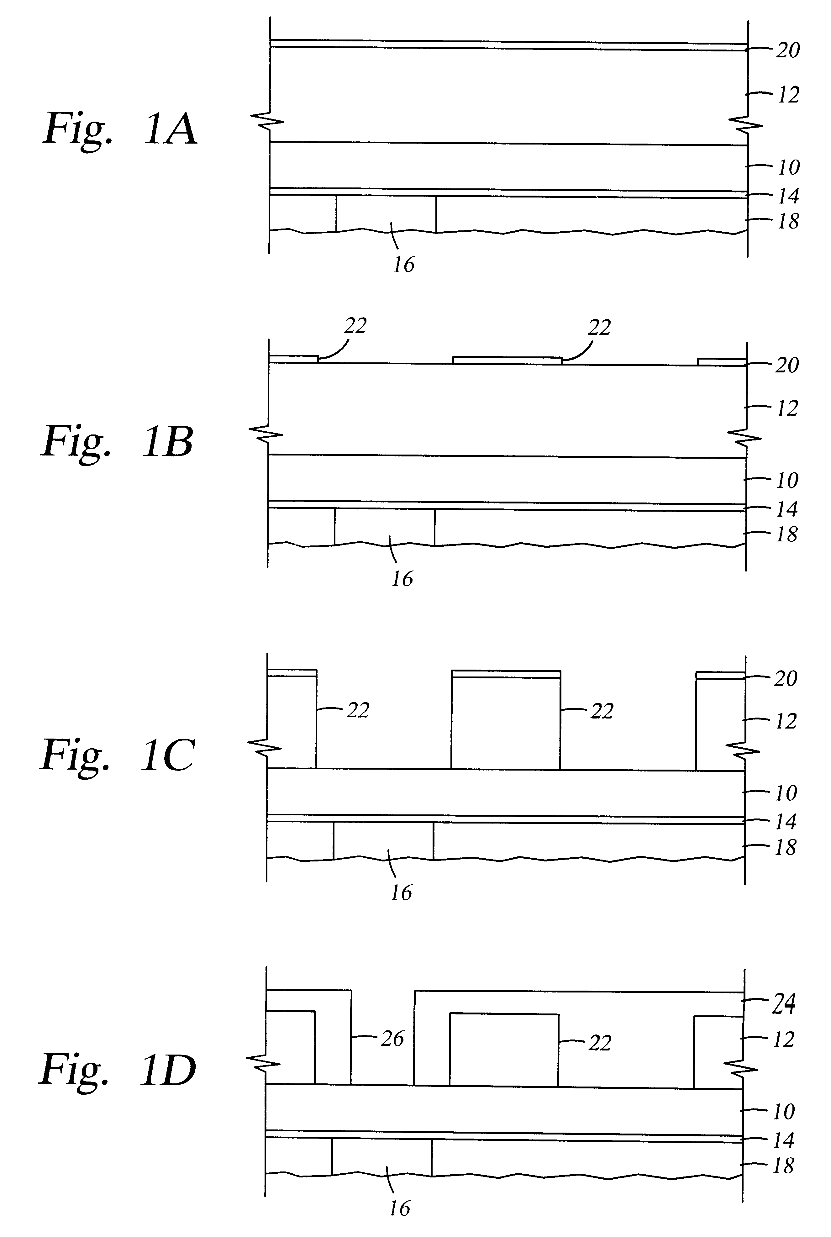
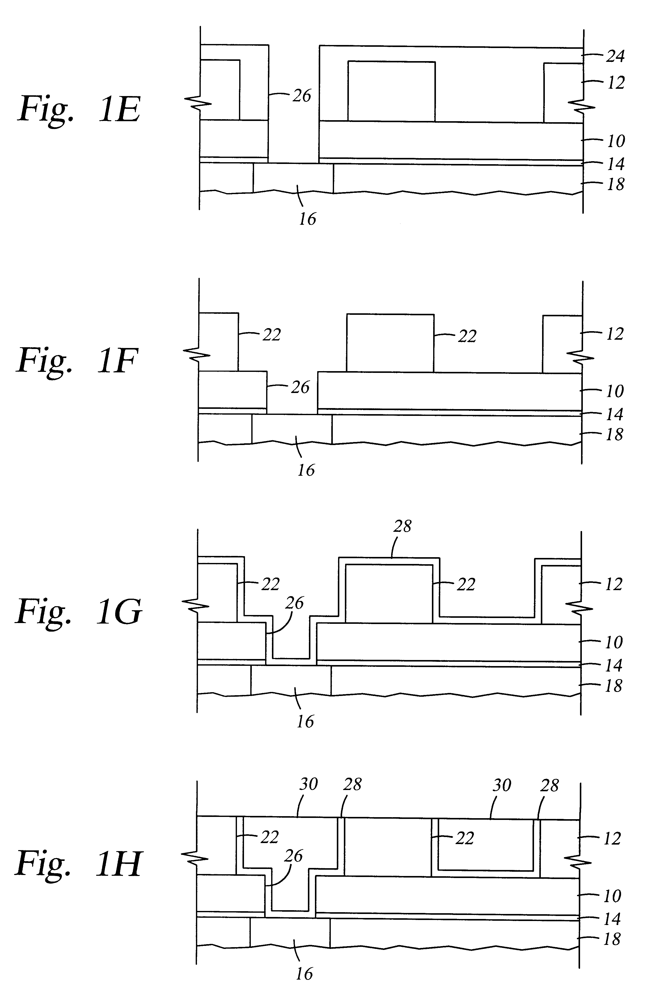
first embodiment
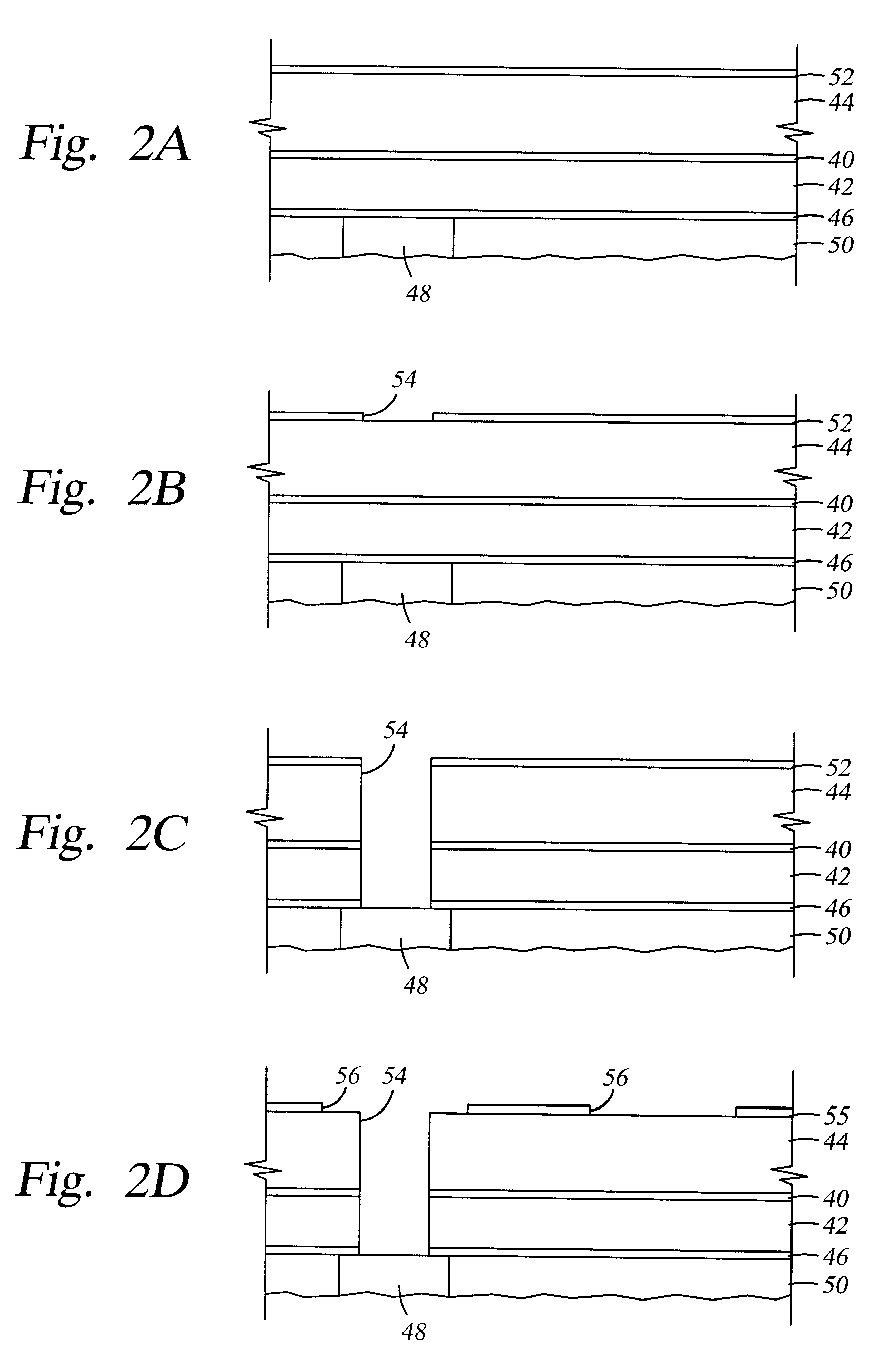
Referring to FIG. 2B, the photoresist 52 hard mask is then patterned to define vertical interconnects 54 to be etched in the first and third low k dielectric layers 42, 44 and the etch stop layer 40. As shown in the first embodiment above, a pattern defining horizontal interconnects could be used first. A typical photoresist for silicon oxide layers is "RISTON," manufactured by duPont de Nemours Chemical Company. The photoresist is exposed to UV light to define the pattern and then portions of the photoresist are stripped away. A hard mask such as a silicon oxide layer containing carbon or hydrogen could be used below the photoresist and etched as described below after the pattern is developed in the photoresist. The photoresist or hard mask then provides the pattern that is transferred to the underlying layers.
Referring to FIG. 2C, the vertical interconnects 54 are then etched into the first and third low k dielectric layers 42, 44, the low k etch stop layer 40, and the barrier lay...
example 1
A first oxidized methylsilane layer is deposited on an 8 inch silicon substrate placed in a DxZ chamber, available from Applied Materials, Inc., at a chamber pressure of 3.0 Torr and temperature of 15.degree. C. from reactive gases which are flowed into the reactor as follows:
The substrate is positioned 320 mil from the gas distribution showerhead and 300 W of high frequency RF power (13 MHz) is applied to the showerhead for plasma enhanced deposition of a first oxidized methylsilane layer containing about 5% carbon by atomic weight and about 0.3% hydrogen by atomic weight, the first layer having a thickness of at least 5,000 .ANG.. Then the flow of methylsilane is increased to 68 sccm and a second oxidized methylsilane layer containing about 10.5% carbon by atomic weight and about 3% hydrogen by atomic weight is deposited at a power level of 80 W, the second layer having a thickness of at least 1000 .ANG.. Then the flow of methysilane is decreased to 34 sccm and deposition of a thi...
example 2
The preceding example deposits the dielectric layers in a single chamber by varying only the flow of the silicon compound and the power level. This example modifies the first example by replacing methylsilane with TEOS for the first dielectric layer as follows.
A first oxidized TEOS layer is deposited on an 8 inch silicon substrate placed in a DxZ chamber, available from Applied Materials, Inc., at a chamber pressure of 3.0 Torr and temperature of 350.degree. C. from reactive gases which are flowed into the reactor as follows:
The substrate is positioned 320 mil from the gas distribution showerhead and 750 W of high frequency RF power (13 MHz) is applied to the showerhead for plasma enhanced deposition of a silicon oxide layer containing less than 1% carbon by atomic weight and less than 0.1% hydrogen by atomic weight, the layer having a thickness of at least 5000 .ANG.. Then deposition of second and third dielectric layers then continues using methysilane as described for Example 1.
E...
PUM
| Property | Measurement | Unit |
|---|---|---|
| dielectric constant | aaaaa | aaaaa |
| feature sizes | aaaaa | aaaaa |
| feature sizes | aaaaa | aaaaa |
Abstract
Description
Claims
Application Information