Mobile ionic contamination detection in manufacture of semiconductor devices

a technology of semiconductor devices and ionic contamination, which is applied in the direction of measurement devices, electronic circuit testing, instruments, etc., can solve the problems of limiting the sensitivity of the test structure, ionic contamination, and the inability to efficiently perform life tests at the time of manufactur

Inactive Publication Date: 2002-02-19
BELL SEMICON LLC
View PDF8 Cites 102 Cited by
  • Summary
  • Abstract
  • Description
  • Claims
  • Application Information

AI Technical Summary

Benefits of technology

It is another object of the present invention to provide an improved method of manufacturing MOS devices in which detection of mobile ionic contamination is more efficient.

Problems solved by technology

Particularly, ionic contamination is an issue in MOS field-effect transistors where the junction between the gate oxide and the underlying silicon channel region is susceptible to this problem.
The time for this contamination to build up to a point where the threshold voltage is noticeably affected is lengthy, however, so a life test cannot be performed in any efficient manner at the time of manufacture.
This narrow width restricts the sensitivity of the test structure.

Method used


Image

  • Mobile ionic contamination detection in manufacture of semiconductor devices
  • Mobile ionic contamination detection in manufacture of semiconductor devices
  • Mobile ionic contamination detection in manufacture of semiconductor devices

Examples


Embodiment Construction

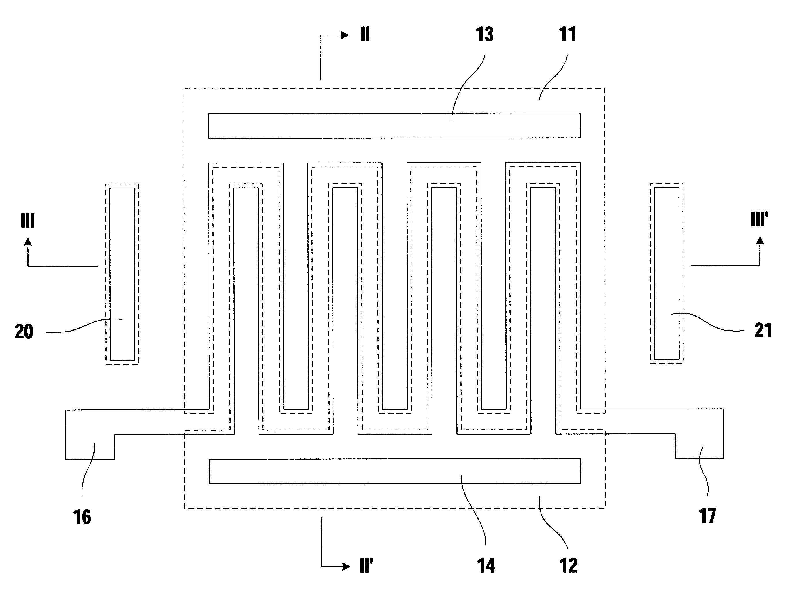
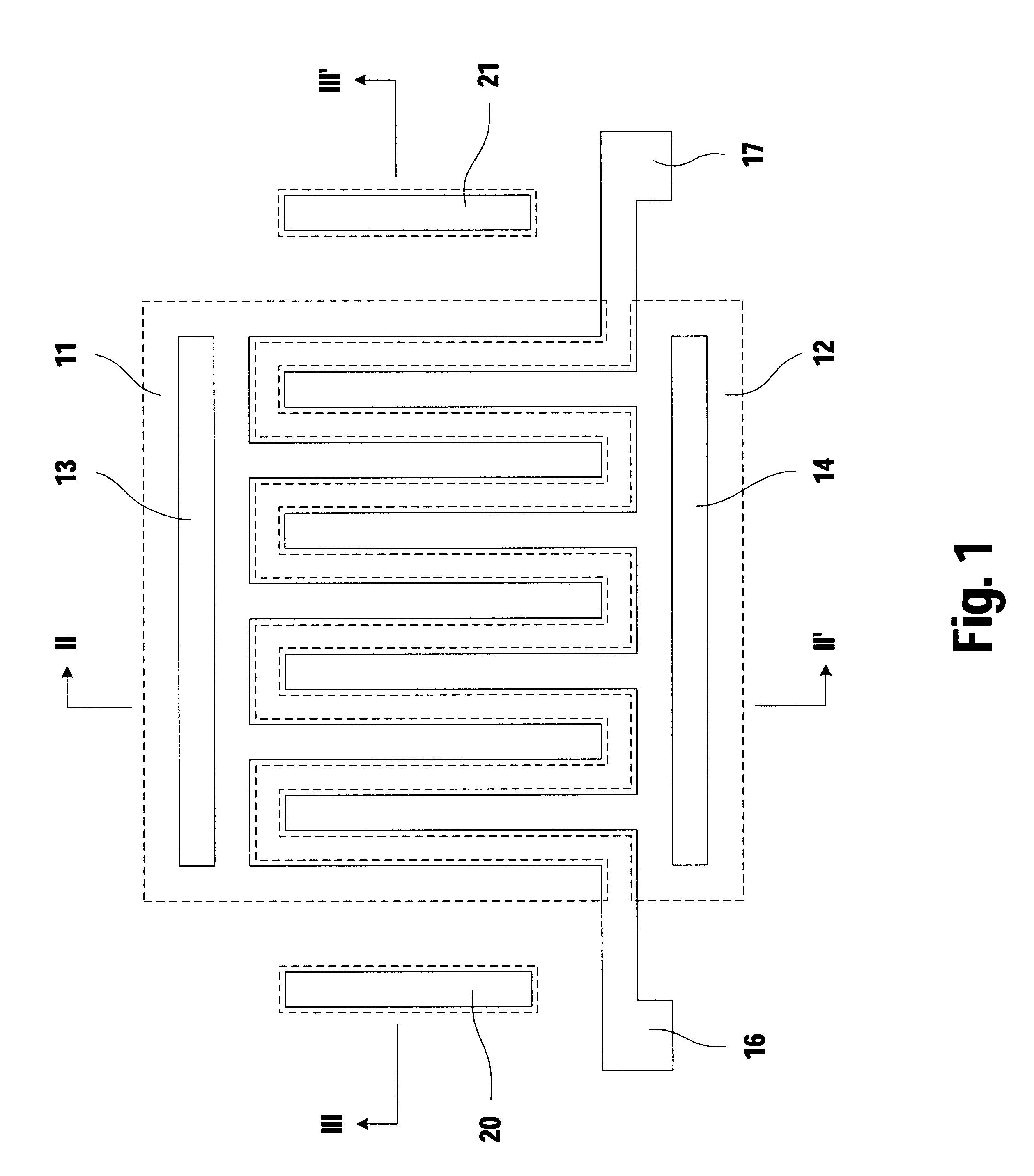
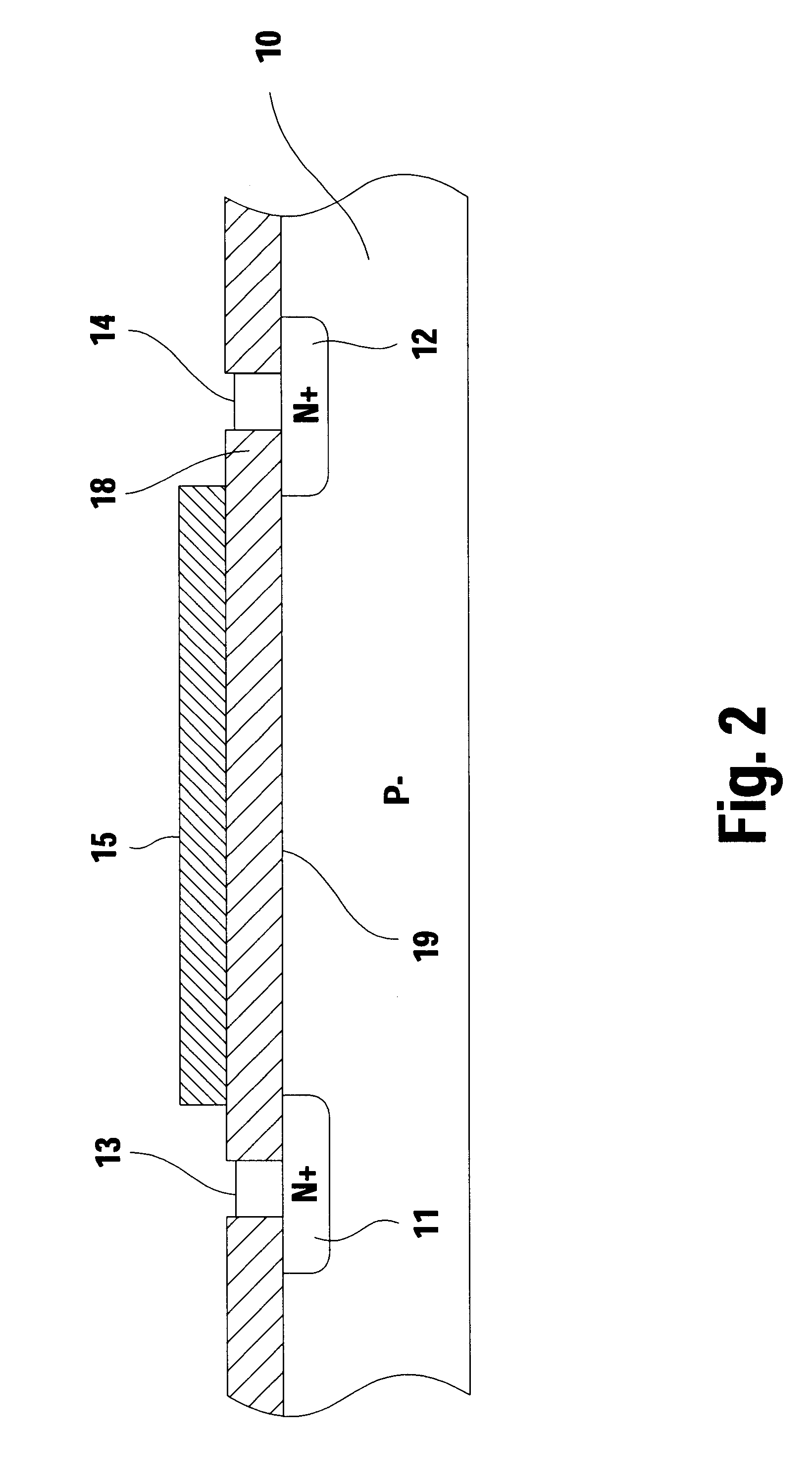
Referring to FIGS. 1, 2, and 3, semiconductor device is shown in plan and section views to illustrate features of the invention. A silicon chip 10 has a test transistor formed therein by N+ source and drain regions 11 and 12, creating a thick-oxide MOS transistor. Metal contacts 13 and 14 provide source and drain connections for testing. The substrate is predominately P- type in this illustrative embodiment. A gate is created by an elongated serpentine metal strip 15 extending between source and drain, with metal pads 16 and 17 at the ends of the strip for applying voltages and currents thereto during the test. Thick field oxide 18 separates the gate 15 from a channel 19 between source 11 and drain 12. The field oxide 18 is many times thicker than gate oxide used for the logic or memory transistors on the chip, and is the same oxide used in peripheral areas of the chip to isolate functional devices from one another. Contact to the substrate region of the chip 10 is made at contact p...


PUM


Abstract

A test transistor structure formed in a semiconductor device has a thick-oxide transistor with an elongated serpentine-shaped metal gate. The gate is used to first measure the threshold voltage of the thick-oxide test structure. Then, a current is passed through the elongated metal line which forms the serpentine gate to heat the area of the test structure. While being heated, a stress voltage is applied between the substrate and one end of the gate electrode, this stress voltage being much larger than the logic voltage used in operating thin-oxide transistors on the chip. After a selected time, the current is removed, the stress voltage is removed, and the threshold voltage of the thick-oxide transistor is again measured and compared to the original value. Any reduction in threshold voltage can be attributed to the migration of positive charge to the silicon-to-oxide interface beneath the gate, and is proportional to the area between the source and drain regions of the test transistor.

Description

1. Technical FieldThis invention relates to semiconductor devices, and more particularly to test structures formed in a surface of a semiconductor device for detecting mobile ionic contamination at a silicon-to-oxide interface, during manufacture.2. Description of the Related ArtIn the manufacture of semiconductor devices, test structures are added to the circuitry on a chip or wafer to facilitate making various tests. One of the qualities for which test data is needed is that of the degree of contamination by mobile ions at a silicon-to-oxide interface. Particularly, ionic contamination is an issue in MOS field-effect transistors where the junction between the gate oxide and the underlying silicon channel region is susceptible to this problem. Whenever an electric field is maintained across a silicon oxide layer for long periods of time, ions of contaminant materials will migrate toward an interface. The time for this contamination to build up to a point where the threshold voltage...

Claims


Application Information

Patent Timeline
Patent Type & Authority Patents(United States)
IPC IPC(8): G01R31/26G01R31/28
CPCG01R31/2858G01R31/2628
Inventor YAKURA, JAMES
Owner BELL SEMICON LLC
Why Eureka
Try Eureka