High conductivity buried layer in optical waveguide

a technology of optical waveguide and conductivity layer, which is applied in the direction of optical waveguide light guide, instruments, optics, etc., can solve the problems of limited circuit configuration possible for controlling the device, the operation bandwidth of devices relying on the plasma dispersion effect, and the use of a substrate base for one of the electrodes

Inactive Publication Date: 2002-04-16
QINETIQ LTD
View PDF4 Cites 79 Cited by
  • Summary
  • Abstract
  • Description
  • Claims
  • Application Information

AI Technical Summary

Problems solved by technology

Conversely, operating bandwidths of devices relying on the plasma dispersion effect in silicon waveguide are restricted by rapidity of removal and injection of charge carriers from a region thereof in which optical radiation propagates; such devices may provide operating bandwidths of several tens of megahertz in practice.
One of these limitations is that the substrate base is used for one of the electrodes.
This results in a first problem when several devices are formed together on the substrate base that the base will form a second electrode common to the devices.
This places limitations on circuit configuration possible for controlling the device.
This results in a second problem of electrode series resistance which degrades device operating efficiency because power is dissipated within the series resistance itself rather than in regions where charge injection occurs and a useful modulation effect is obtained.
However, radiation propagates predominantly in a central region of the ...

Method used


Image

  • High conductivity buried layer in optical waveguide
  • High conductivity buried layer in optical waveguide
  • High conductivity buried layer in optical waveguide

Examples


Embodiment Construction

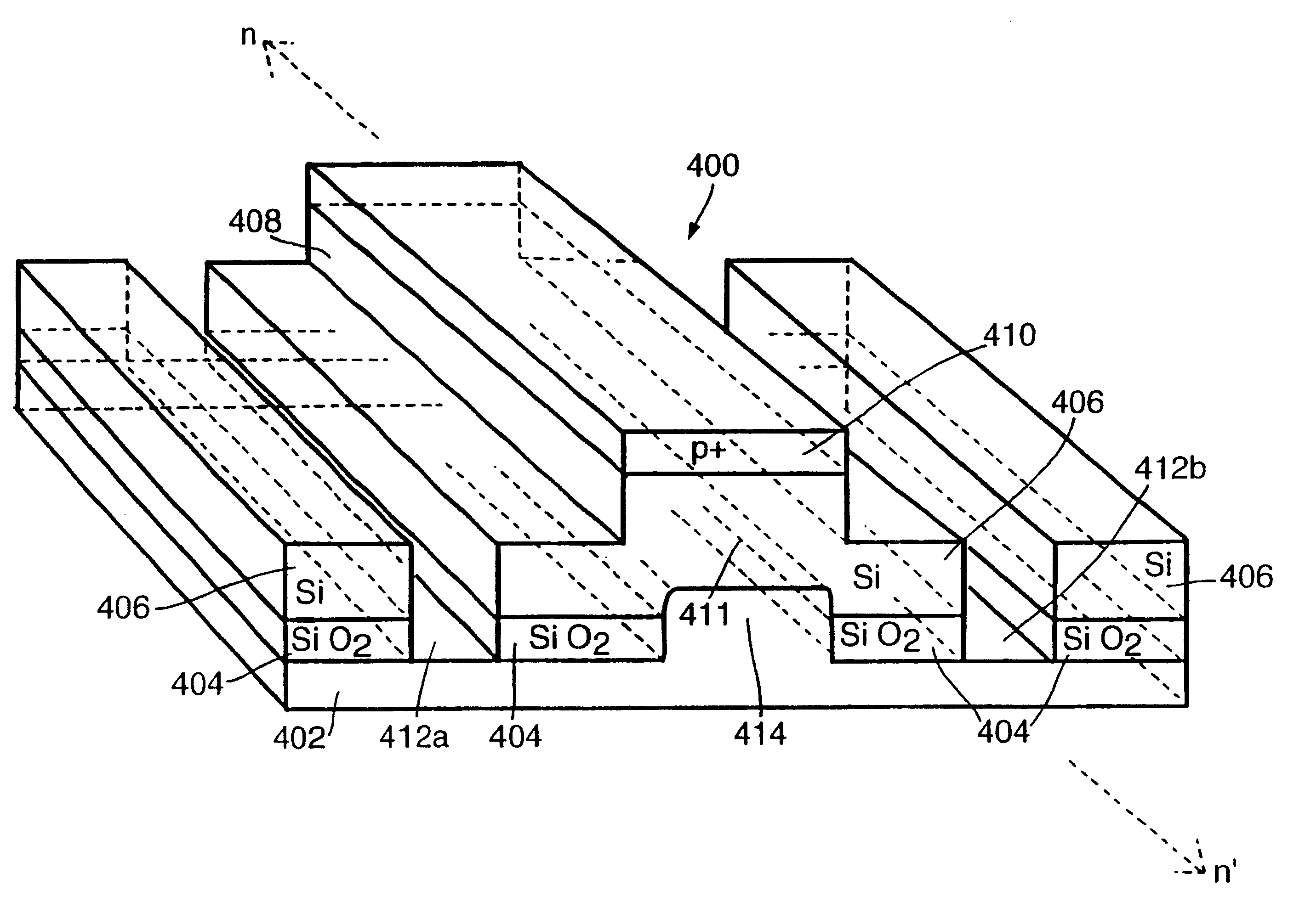
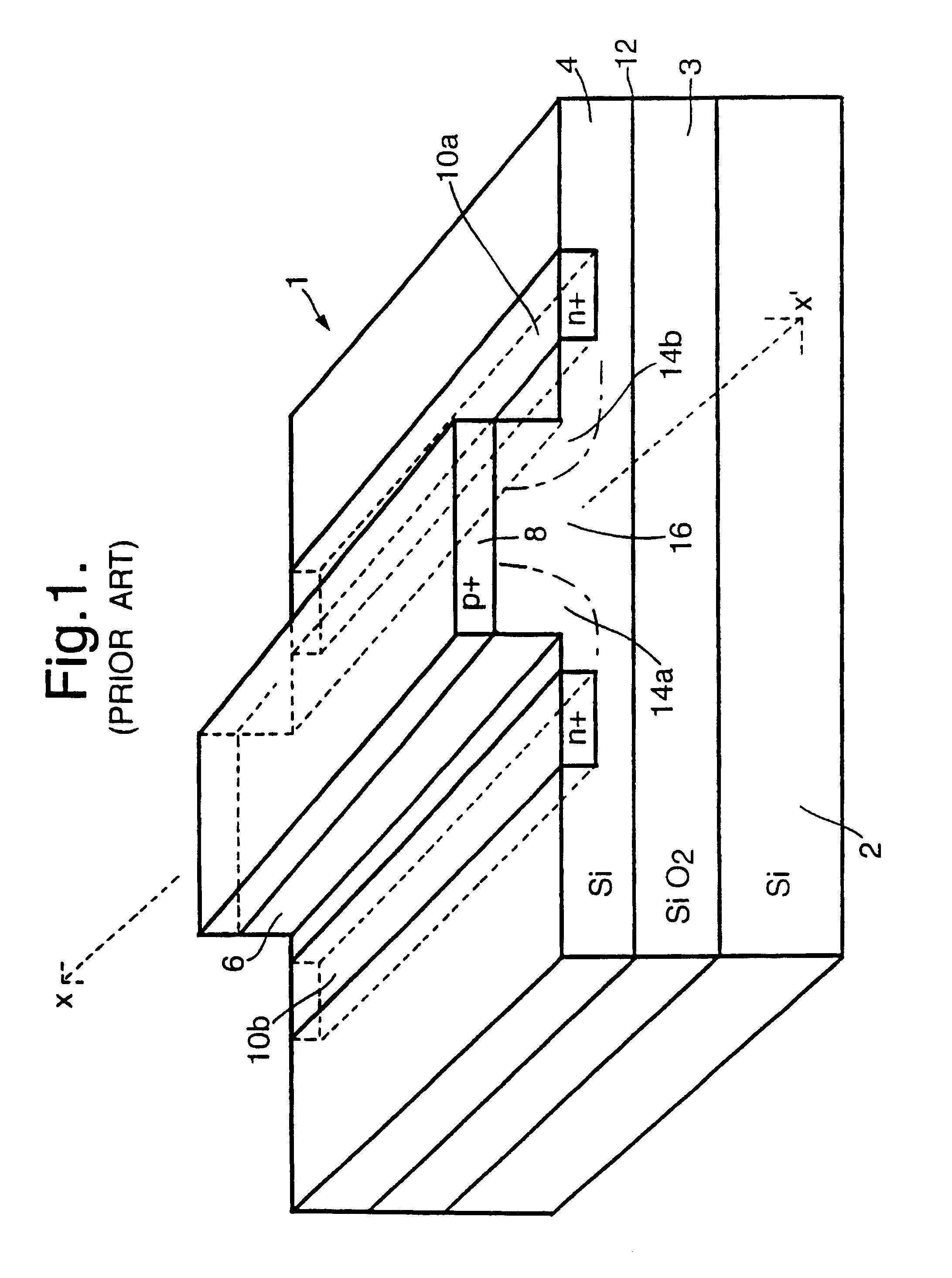
Referring to FIG. 1, there is shown a schematic view of a prior art plasma dispersion optical modulator device indicated generally by 1. It incorporates in sequence a silicon substrate 2, a silicon dioxide (SiO.sub.2) layer 3 and a silicon surface layer 4. The substrate 2, the silicon dioxide layer 3 and the surface layer 4 are parallel, overlaid and unitary. The surface layer 4 is low doped silicon having an impurity concentration of less than 10.sup.16 atoms cm.sup.-3.

The surface layer 4 is etched back during fabrication of the device 1 to form an exposed rib 6. A reference axis x-x' is included in FIG. 1 and is orientated in a direction along the rib 6. The rib 6 is doped along its upper surface to form an elongate p+ electrode 8 thereonto. An exposed surface of the surface layer 4 is doped to form two elongate n+ electrodes 10a, 10b into the surface layer 4. The n+ electrodes 10a, 10b are adjacent at respective sides of the rib 6 but do not encroach onto it. The p+ electrode 8, ...


PUM


Abstract

An optical device (300) comprises a multilayer structure, formed by wafer bonding, incorporating in sequence a silicon dioxide layer (304), a buried silicide layer (306), a contact layer (308) and a silicon surface layer (310). The surface layer (310) is selectively etched to form an exposed rib (312). An upper surface of the rib (312) is doped to form an elongate electrode (314) therealong. The surface layer (310) is selectively etched to the contact layer (308) in regions remote from the rib (312) to form via channels (316a, 316b) for making electrical connection to the contact layer (308). The rib (312) forms a waveguide along which radiation propagates. When the electrode (314) is biased relative to the contact layer (308), charge carriers are injected into the rib (312) and induce refractive index changes in a central region (324) thereof where most of the radiation propagates along the rib (312). The silicide layer (306) provides an efficient current conduction path for injecting the carriers, thereby providing enhanced device operating bandwidth and reduced power dissipation.

Description

1. Field of the InventionThis invention relates to an optical device, and particularly but not exclusively to a device for modulating radiation guided in a waveguide.2. Discussion of Prior ArtOptical devices are well known in the prior art. They are described in a publication "Introduction to Semiconductor Integrated Optics" by H P Zappe (ISBN 0-89006-789-9, Artech House Publishers 1995). Optical devices for modulating radiation operate by exploiting optical properties of a modulating medium which are modifiable by external influences. One of the optical properties may include a refractive index. Induced changes in the refractive index may be anisotropic, where the medium becomes birefringent, or isotropic. There are many possible techniques for modulating the refractive index. These techniques are herewith described.Refractive index changes may be induced in some optically transmissive materials by the application of an external mechanical force to them. This is referred to as a ph...

Claims


Application Information

Patent Timeline
IPC IPC(8): G02F1/01G02F1/025
CPCG02F1/025
Inventor BOZEAT, ROBERT JNAYAR, VISHAL
Owner QINETIQ LTD
Why Eureka
Try Eureka