Method of crystallizing a silicon film and thin film transistor and fabricating method thereof using the same

Inactive Publication Date: 2002-05-14
LG DISPLAY CO LTD
View PDF6 Cites 37 Cited by
  • Summary
  • Abstract
  • Description
  • Claims
  • Application Information

AI Technical Summary

Benefits of technology

The present invention therefore improves the characteristics of a silicon film by means of lengthening the time that th

Problems solved by technology

Unfortunately, protruding silicon regions (caused by the collision of silicon grains grown during crystallization) are generated on the surface of the active layer 15.
The grain boundaries protruding out of the surface of the active layer 15 deteriorates step coverage of the gate insulating layer as well as t

Method used


Image

  • Method of crystallizing a silicon film and thin film transistor and fabricating method thereof using the same
  • Method of crystallizing a silicon film and thin film transistor and fabricating method thereof using the same
  • Method of crystallizing a silicon film and thin film transistor and fabricating method thereof using the same

Examples


first embodiment

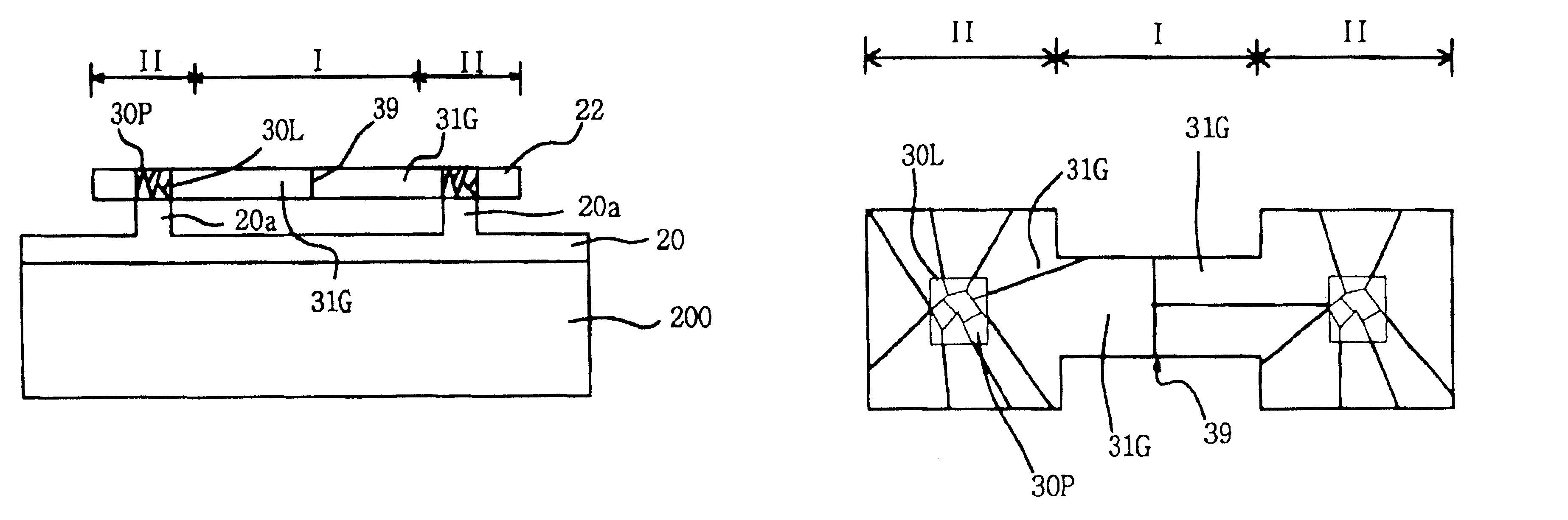
FIG. 2A to FIG. 2E are cross-sectional views illustrating crystallization of a silicon film according to the present invention, and FIG. 3A to FIG. 3E are corresponding plan views of the silicon film patterns shown in FIG. 2A to FIG. 2E.

Referring to FIG. 2A and FIG. 3A, after a buffer layer 20 has been formed on an insulating layer 200, an amorphous silicon film 21 is deposited on the buffer layer 20.

The buffer layer 20 is formed of a substance having a thermal conductivity higher than that of air, such as an oxide layer.

Referring to FIG. 2B and FIG. 3B, an amorphous silicon film pattern 22 having a predetermined shape is formed by patterning the amorphous silicon film 21 by, for example, photolithography.

The predetermined shape includes a first region I of a first size and second regions 11, as seen in FIG. 3B.

As shown in the drawings, the first region I lies at the center of the silicon film pattern 22 and has a first dimension `d1`, and the rectangular second regions 11 each have...

second embodiment

the present invention relies on sequential lateral crystallization using multiple applications of laser energy irradiated with a predetermined overlapping ratio, while the first embodiment uses a single application of laser energy.

Sequential lateral crystallization, which takes advantage of the fact that silicon grains grow perpendicularly to an interface between the liquid silicon and the solid silicon regions, has grains grow laterally to predetermined lengths by suitably manipulating the magnitude of laser energy used and the irradiation displacement of a laser beam properly (Robert S. Sposilli, M. A. Crowder, and James S. Im, Mat. Res. Soc. Symp. Proc. Vol. 452, 956-957, 1997).

The following drawings show only a silicon film pattern for the convenience of description.

Referring to FIG. 4A, as explained in the first embodiment of the present invention, a first laser beam irradiation is carried out on a patterned amorphous silicon film pattern but the laser beam pattern has a width ...

third embodiment

FIG. 5A and FIG. 5B are plan views illustrating crystallization of a silicon film according to the present invention.

Referring to FIG. 5A, an amorphous silicon film pattern 51 comprises a first region I and a pair of second regions II. The first region I has a first dimension `d1` from a side of region I to an imaginery axis bisecting region I. Each of the second regions II have a second dimension `d2` from a central part thereof to an edge, which is longer than `d1`. Each region II has a triangular shape with a vertex directed to the first region I. The second regions II are connected to both ends of the first region I.

As described in the first embodiment of the present invention, a buffer layer under the amorphous silicon film pattern 51 is overetched, thereby forming a space contact region 51-1 and triangular shaped buffer contact regions 51-2 in the amorphous silicon film pattern 51.

Referring to FIG. 5B, the result of the laser crystallization is the same as in the first embodim...


PUM

PropertyMeasurementUnit
Timeaaaaaaaaaa
Energyaaaaaaaaaa
Thermal conductivityaaaaaaaaaa

Abstract

The present invention relates to a method of crystallizing a silicon film, a thin film transistor, and a fabricating method thereof using the same. More particularly, the present invention relates forming a crystalline silicon film by crystallizing a silicon film using laser energy, and a thin film transistor and a fabricating method thereof using the same. The present invention includes forming a buffer layer on a substrate and forming an amorphous silicon film on the buffer layer wherein the amorphous silicon film includes a first region and second regions connected to both ends of the first region. The buffer layer is etched to a degree by using the amorphous silicon as a mask, wherein a space is formed under the first region and a central part of the second region contacts a remaining portion of the buffer layer. The amorphous silicon film is then crystallized. In another aspect, the present invention includes a method of fabricating a thin film transistor using this method of crystallizing an amorphous silicon film.

Description

BACKGROUND OF THE INVENTION1. Field of InventionThe present invention relates to a method of crystallizing a silicon film, a thin film transistor, and a fabricating method for a thin film transistor. More particularly, the present invention relates to a method for crystallizing a silicon film using laser energy, a thin film transistor, and a fabricating method for a thin film transistor using laser energy.2. Discussion of Related ArtSilicon can be crystallized by using laser energy to melt amorphous silicon and extracting silicon crystals by cooling down or solidifying the fused silicon. In this case, monocrystalline silicon is formed if the growing direction of silicon is uniform relative to the growth of grains. Otherwise, polycrystalline silicon is formed when a plurality of crystals grow randomly and simultaneously.When an active layer of a thin film transistor (hereinafter abbreviated TFT) is formed by crystallizing an amorphous silicon layer, TFT characteristics are improved b...

Claims


Application Information

Patent Timeline
IPC IPC(8): H01L21/02H01L29/786H01L21/336H01L29/66H01L21/20H01L21/268
CPCH01L21/2026H01L27/1281H01L29/78675H01L29/66757H01L21/02488H01L21/02532H01L21/02675H01L21/268
Inventor YI, JONGHOONLEE, SANGGUL
Owner LG DISPLAY CO LTD
Why Eureka
Try Eureka