Methods for fabricating memory devices

a memory device and floating gate technology, applied in the field of memory devices having multi-dot floating gate fabrication, can solve the problems of limited integration of the semiconductor memory based on such constitution, requiring a larger cost and longer process time,

Inactive Publication Date: 2002-06-25
SONY CORP
View PDF7 Cites 28 Cited by
  • Summary
  • Abstract
  • Description
  • Claims
  • Application Information

AI Technical Summary

Benefits of technology

According to the present invention, a laser with a high pulse energy density is used in the first laser annealing in which a large laser pulse energy density is required for polycrystallizing the silicon film, and a laser with an pulse energy density lower than that used in the first laser annealing is used in the second laser annealing in which not so large pulse energy density is required for forming the semiconductor dots. Since the laser anneal conditions are optimally selected individually in the first and second laser annealings, the semiconductor film can be polycrystallized in a desired manner, and semiconductor dots can desirably be dispersed within the semiconductor dot forming film to be provided as semiconductor dots. In this process, the tunnel oxide film is successfully prevented from being damaged by stress caused by the polycrystallization of semiconductor or by the laser annealing with a large pulse energy density. When the flatness of the surface of the polycrystallized semiconductor film is not sufficient, a desirable flatness can be obtained by, for example, the CMP (chemical mechanical polishing) process.

Problems solved by technology

The semiconductor memories based on such constitution have, however, been suffering from a limited degree of integration.
The conventional floating gate MOS memory is, however, disadvantageous in that it requires a larger cost and longer process time since the silicon dots (silicon thin wires) are formed by photolithography and then shrunk by thermal oxidation (back thermal oxidation) process at high temperatures.
The problem also resides in that such heat treatment at high temperatures makes it difficult to fabricate the memory device when the substrate thereof is made of glass or plastic.
In the method disclosed in Japanese Patent Application Publication No. 11-274420, in which the silicon film is converted into the polysilicon film by a single process of the laser annealing, and at the same time the SiO.sub.x film is decomposed to produce stoichiometric SiO.sub.2 and Si thereby to obtain the silicon dots, a problem resides in that the surface flatness of the polycrystallized silicon layer undesirably ruined by the laser annealing cannot be recovered, and in that a tunnel oxide film may be damaged due to stress caused by shrinkage during the polycrystallization of silicon and the laser annealing with a high-output laser.
It was also observed that the silicon film is not sufficiently polycrystallized while the silicon dots are successfully formed, or on the contrary the silicon film is sufficiently polycrystallized while the silicon dots are destroyed.

Method used


Image

  • Methods for fabricating memory devices
  • Methods for fabricating memory devices
  • Methods for fabricating memory devices

Examples


example

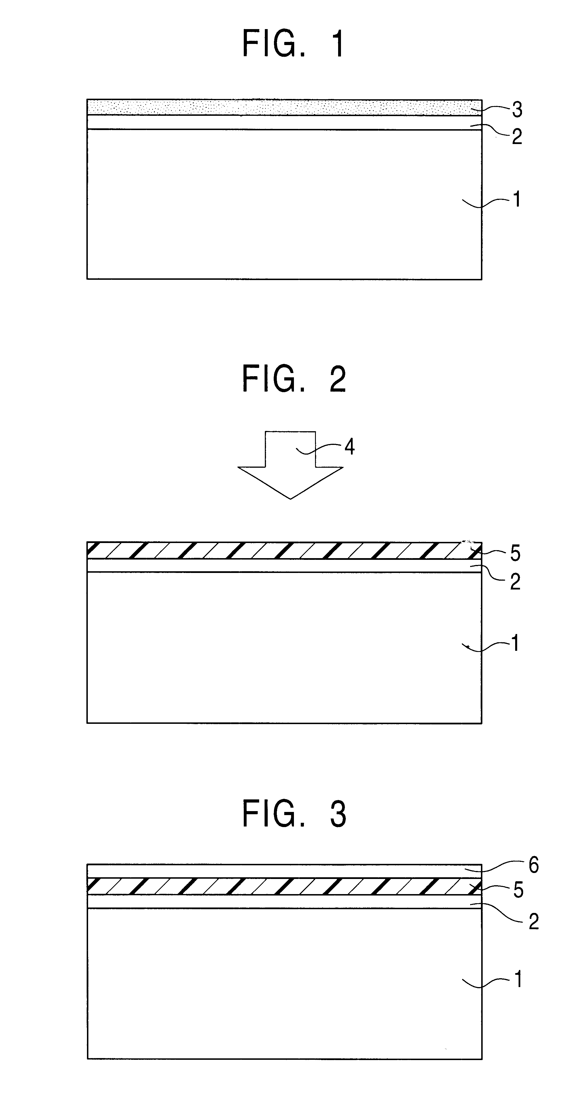
On the surface of a quartz substrate of 500 .mu.m thick, an SiO.sub.2 film of 200 nm thick was formed by the PECVD process.

Next, a hydrogenated amorphous silicon film was formed on the SiO.sub.2 film by the PECVD process, and then dehydrogenated by keeping the film within a vacuum chamber conditioned at 10.sup.-6 Torr and 400.degree. C. for 2 hours, thereby to form an Si film of 30 nm thick.

Next, XeCl excimer laser beam with a pulse width of 30 nsec and a pulse energy density of 300 mJ / cm.sup.2 (wavelength=308 nm) was irradiated as much as 100 shots on the surface of the Si film, thereby to effect the laser annealing. By such laser annealing, the Si film was polycrystallized and thus a polysilicon film was formed.

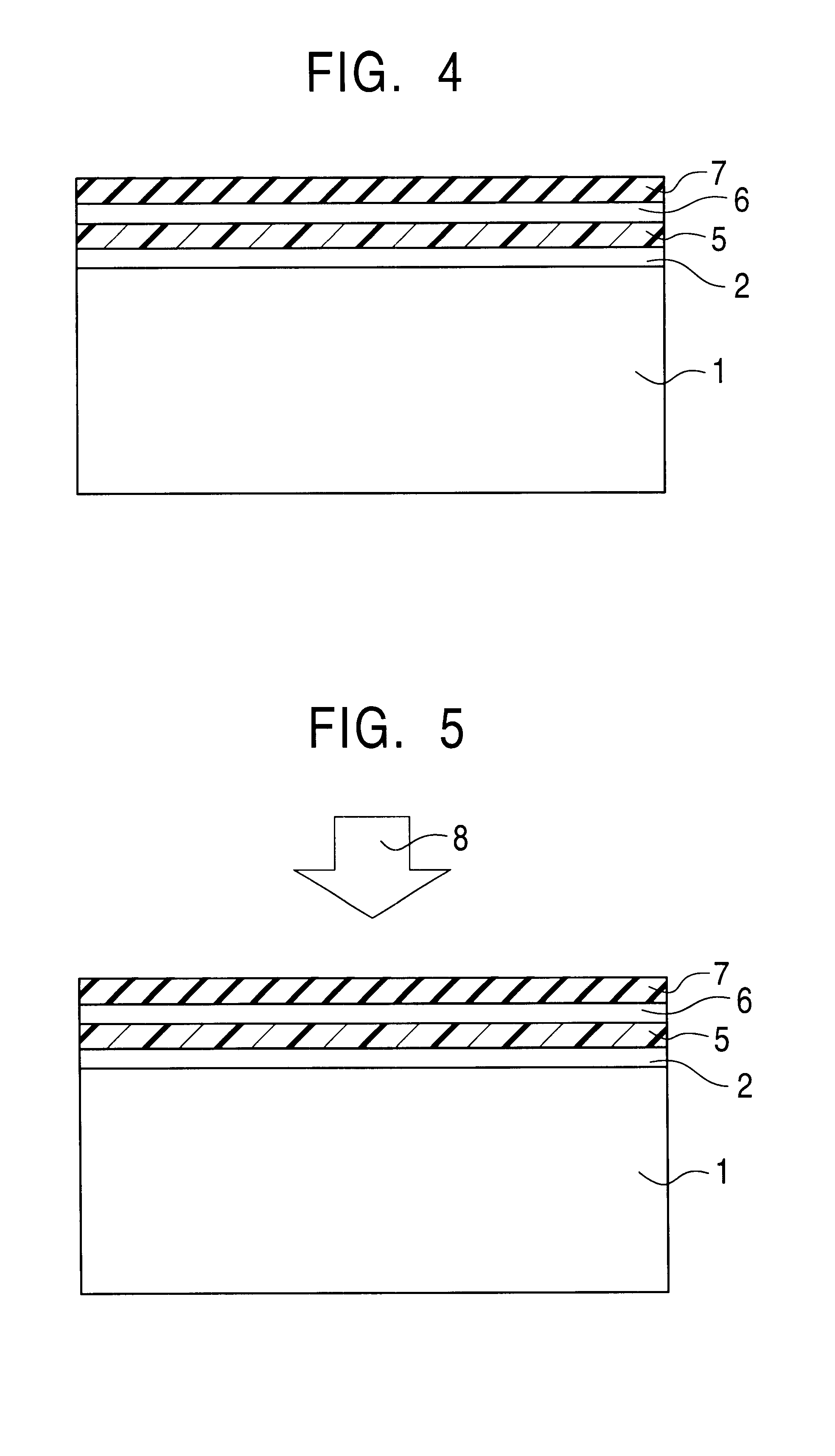
Next, a tunnel SiO.sub.2 film of 10 nm thick was formed on the polysilicon film by the PECVD process.

Next, on the tunnel SiO.sub.2 film, a Si-excessive non-stoichiometric SiO.sub.x film (x=1.59) was formed by the PECVD process using SiH.sub.4 gas at a flow rate of 10 SCCM a...


PUM


Abstract

Methods for fabricating memory devices having a multi-dot floating gate ensuring a desirable crystallization of a semiconductor film without ruining the flatness of the surface of the polycrystallized silicon layer and a tunnel oxide film, allowing desirable semiconductor dots to be produced, and allowing production of the memory devices having a multi-dot floating gate with ease and at low costs even when a substrate is made of glass or plastic. Such a method for fabricating memory devices includes steps for forming on a substrate a semiconductor film and treating said semiconductor film by a first laser annealing so as to have a polycrystalline structure; forming on the semiconductor film a semiconductor dot forming film having a non-stoichiometric composition with an excessive content of a semiconductor element; and dispersing semiconductor dots within the semiconductor dot forming film by a second laser annealing thereby to produce semiconductor dots; in which a pulse energy density of the laser used for the first laser annealing is larger than a pulse energy density of the laser used for the second laser annealing.

Description

RELATED APPLICATION DATAThe present application claims priority to Japanese Application No. P11-261969 filed Sep. 16, 1999, which application is incorporated herein by reference to the extent permitted by law.1. Field of the InventionThe present invention relates to methods for fabricating memory devices having a multi-dot floating gate, and in more detail to methods for fabricating memory devices ensuring a desirable crystallization of a semiconductor film without ruining the surface flatness of the polycrystallized silicon layer and a tunnel oxide film, allowing desirable semiconductor dots to be produced, and allowing production of the memory devices having multi-dot floating gate with ease and at low costs even when a substrate is made of glass or plastic.2. Description of Related ArtIn recent years, degree of integration of semiconductor memory devices such as DRAM (dynamic random access memory) and SRAM (static random access memory) keeps on increasing. Such semiconductor memo...

Claims


Application Information

Patent Timeline
Patent Type & Authority Patents(United States)
IPC IPC(8): H01L21/4763H01L29/786H01L21/02H01L21/70H01L27/115H01L21/336H01L29/66H01L21/8247H01L29/788H01L21/28H01L29/423H01L29/792
CPCB82Y10/00H01L21/28273H01L29/66757H01L29/7881H01L29/42332Y10S438/927H01L29/40114
Inventor TAIRA, KENICHIKAWASHIMA, NORIYUKINOGUCHI, TAKASHIGOSAIN, DHARAM PALUSUI, SETSUO
Owner SONY CORP
Why Eureka
Try Eureka