
Silicone polymer insulation film on semiconductor substrate and method for forming the film

a technology of silicon polymer and insulation film, which is applied in the direction of thermal insulation devices, coatings, chemical vapor deposition coatings, etc., can solve the problems of poor adhesion with silicon-containing materials, low thermal stability of fluorinated amorphous carbon films, and impede high-speed operations, etc., to achieve high humidity resistance, low dielectric constant, and high thermal stability

Inactive Publication Date: 2002-08-13
ASM JAPAN
View PDF11 Cites 135 Cited by
  • Summary
  • Abstract
  • Description
  • Claims
  • Application Information

AI Technical Summary

Benefits of technology

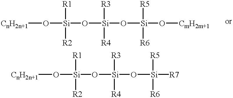
In this method, the material gas is, in short, a silicon-containing hydrocarbon compound including at least one Si--O bond, at most two O--C.sub.n H.sub.2n+1 bonds and at least two hydrocarbon groups bonded to the silicon (Si). Also, this material gas is vaporized by a direct vaporization method. The method results in an insulation film having a low dielectric constant, high thermal stability and high humidity-resistance.
More specifically, the material gas vaporized by the direct vaporization method can stay in the plasma for a sufficient length of time. As a result, a linear polymer can be formed so that a linear polymer having the basic structure (formula 7), wherein the "n" is 2 or a greater value, forms in a vapor phase. The polymer is then deposited on the semiconductor substrate and forms an insulation film having a micropore porous structure. ##STR8##
wherein X1 and X2 are O.sub.n C.sub.m H.sub.p wherein n is 0 or 1, m and p are integers including zero.
The insulation film of this invention has a relatively high stability because its fundamental structure has the Si--O bond having high bonding energy therebetween.

Problems solved by technology

In these multi-layered structures, however, capacitance among individual wires hinders high speed operations.
First, the fluorinated amorphous carbon film has lower thermal stability (370.degree. C.
), poor adhesion with silicon-containing materials and also lower mechanical strength.
The lower thermal stability leads to damage under high temperatures such as over 400.degree. C.
Poor adhesion may cause the film to peel off easily.
Further, the lower mechanical strength can jeopardize wiring materials.
As a result, the dielectric constant of the film cannot be reduced to a desired degree.
As a result, the material gas cannot stay in the reaction chamber for a sufficient length of time to cause polymerization in a vapor phase.
Further, the SOG insulation film of the spin-coat method has a problem in that the material cannot be applied onto the silicon substrate evenly and another problem in which a cure system after the coating process is costly.

Method used


Image

  • Silicone polymer insulation film on semiconductor substrate and method for forming the film
  • Silicone polymer insulation film on semiconductor substrate and method for forming the film
  • Silicone polymer insulation film on semiconductor substrate and method for forming the film

Examples


example 1

Material gas: PM-DMOS (100 sccm)

Additive gases: Ar (140 sccm) and He (140 sccm)

Total flow volume of reaction gas: 480 sccm

Other conditions and devices used for forming the film are given above. The calculated value of the residence time Rt was 103 msec. The conditions in this example reduced the dielectric constant .di-elect cons. of the insulation film to 3.10.

example 2

Material gas: PM-DMOS (100 sccm)

Additive gases: Ar (100 sccm) and He (100 sccm)

Total flow volume of reaction gas: 300 sccm

Other conditions and devices used for forming the film are given above. The calculated value of the residence time Rt was 165 msec. The conditions in this example reduced the dielectric constant .di-elect cons. of the insulation film to 2.76.

example 3

Material gas: PM-DMOS (100 sccm)

Additive gases: Ar (70 sccm) and He (70 sccm)

Total flow volume of reaction gas: 240 sccm

Other conditions and devices used for forming the film are given above. The calculated value of the residence time Rt was 206 msec. The conditions in this example reduced the dielectric constant .di-elect cons. of the insulation film to 2.64.


PUM

PropertyMeasurementUnit
Timeaaaaaaaaaa
Timeaaaaaaaaaa
Timeaaaaaaaaaa

Abstract

A method for forming a silicone polymer insulation film having low relative dielectric constant, high thermal stability and high humidity-resistance on a semiconductor substrate is applied to a plasma CVD apparatus. The first step is vaporizing a silicon-containing hydrocarbon compound expressed by the general formula SialphaObetaCxHy (alpha=3, beta=3 or 4, x, and y are integers) and then introducing the vaporized compound to the reaction chamber of the plasma CVD apparatus. The next step is introducing additive gas into the reaction chamber. The residence time of the material gas is lengthened by reducing the total flow of the reaction gas, in such a way as to formed a silicone polymer film having a micropore porous structure with low relative dielectric constant.

Description

1. Field of the InventionThis invention relates generally to a semiconductor technique and more particularly to a silicone polymer insulation film on a semiconductor substrate and a method for forming the film by using a plasma CVD (chemical vapor deposition) apparatus.2. Description of Related ArtBecause of the recent rise in requirements for the large-scale integration of semiconductor devices, a multi-layered wiring technique attracts a great deal of attention. In these multi-layered structures, however, capacitance among individual wires hinders high speed operations. In order to reduce the capacitance it is necessary to reduce the dielectric constant (relative permittivity) of the insulation film. Thus, various materials having a relatively low dielectric constant have been developed for insulation films.Conventional silicon oxide films SiO.sub.x are produced by a method in which oxygen O.sub.2 or nitrogen oxide N.sub.2 O is added as an oxidizing agent to a silicon material gas...

Claims


Application Information

Patent Timeline
IPC IPC(8): B05D7/24C09D4/00C23C16/40H01L21/02H01L21/312
CPCB05D1/62C09D4/00C23C16/401H01L21/02126H01L21/02216H01L21/02274H01L21/3122C08G77/00
Inventor MATSUKI, NOBUO
Owner ASM JAPAN
Learn More