Method of electroless plating copper on nitride barrier

a technology of nitride barrier and electroless plating, which is applied in the direction of conductive pattern formation, liquid/solution decomposition chemical coating, and insulating substrate metal adhesion improvement, etc., can solve the problems of controlling the plating process, complex chemical reactions occurring at the plated surface, and limited acceptance of the technology in the ic manufacturing community

Inactive Publication Date: 2002-08-20
TAIWAN SEMICON MFG CO LTD
View PDF29 Cites 339 Cited by
  • Summary
  • Abstract
  • Description
  • Claims
  • Application Information

AI Technical Summary

Problems solved by technology

Although electroless plating-based processes, such as contact-hole filling, offer many advantages to the process designer, the technique has only found limited acceptance within the IC manufacturing community.
Although the technique appears to be relatively simple, the chemical reactions occurring at the plated surface can be complex.
Some of the factors inhibiting the wider application of electroless plating are the difficulties in controlling the plating process and in obtaining uniform plating thickness on the entire substrate, as well as the sensitivity to contaminants exhibited by the process.
Many of these problems are related to the previously known surface activation techniques, i.e., methods used to render the plated surface catalytically active.
This low activity has a significant detrimental impact on the uniformity of structures formed by this process and on the resulting yield.
Features that are small or separated with large distances from other features are significantly more difficult to plate.
The presence of such particles may result from a contamination of the plating bath with the airborne dust.
It is intuitively clear, however, that any mechanism that prevents undesirable auto-catalytic plating on small particles in the bath may also impede the desirable plating of small, isolated features pre...

Method used


Image

  • Method of electroless plating copper on nitride barrier
  • Method of electroless plating copper on nitride barrier
  • Method of electroless plating copper on nitride barrier

Examples


Embodiment Construction

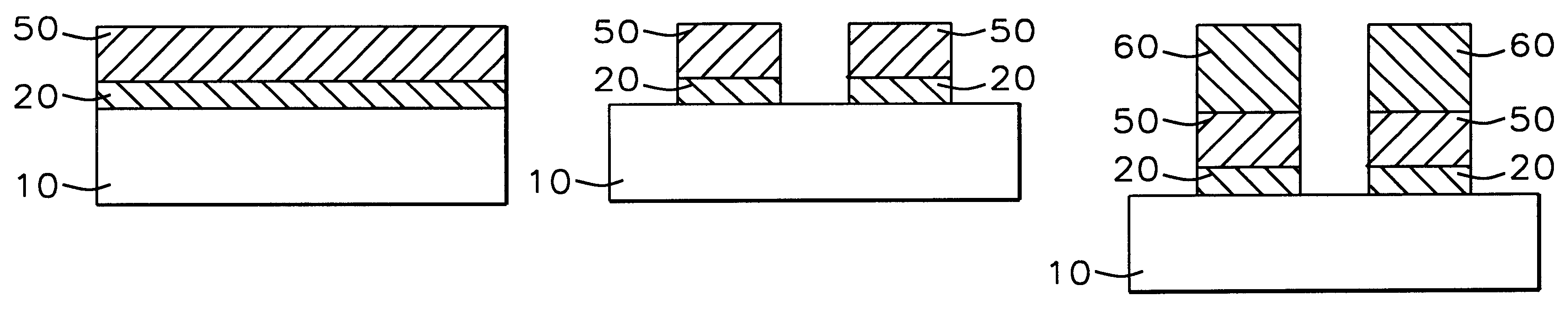
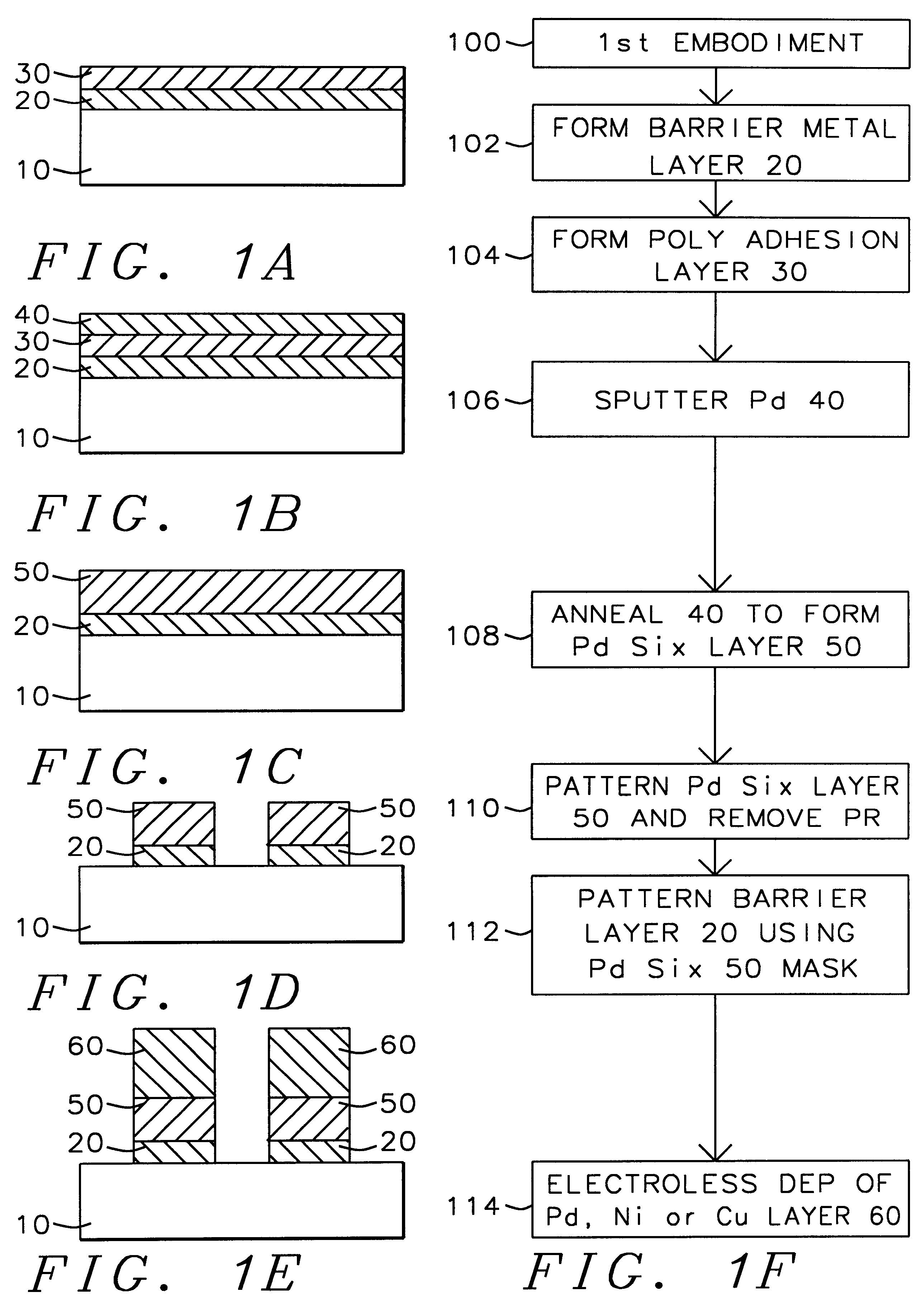
The invention has 3 preferred embodiments. The first embodiment forms metal lines or interconnects. The key features / steps of the first embodiment are: step 108--PdSix layer 50 The table below indicates the key steps and their importance.

The 1st embodiment solves the problems of: forming the silicide layer on the surface of refractory metal or contact hole and then the electroless plating can easily selectively deposited metal on the exposed PdSix region.

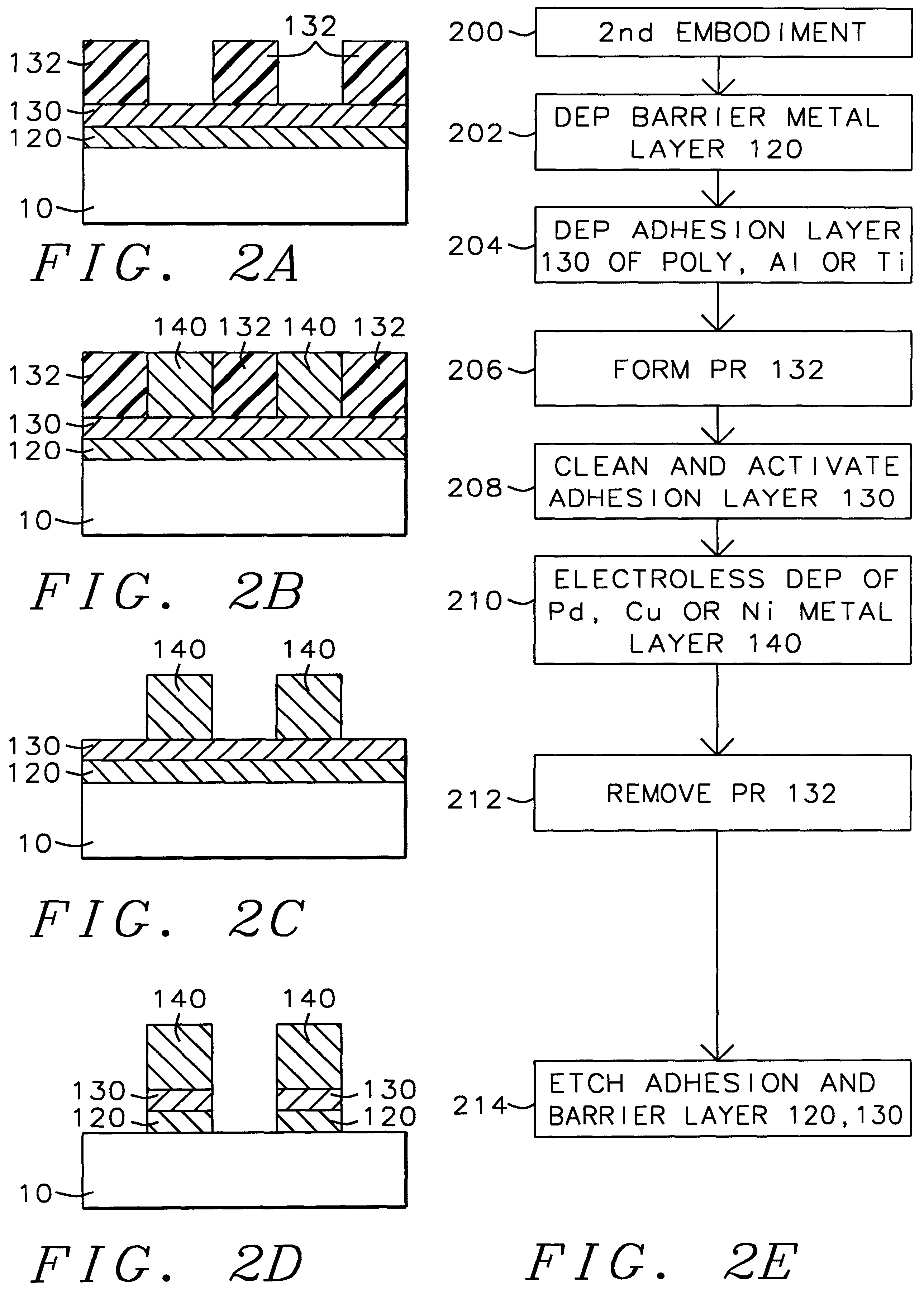
The second embodiment forms another metal line. The key features / steps of the second embodiment are:

The second embodiments using Al, Poly or Ti material as a seed material, (Adhesion layer 130). The metal is selectively electroless deposited over the adhesion layer. Also important is the pickeling and activating or zincating process. The 2nd embodiment is very simple and compatible with conventional IC processing.

The third embodiment forms a solder bump. The key features / steps of the third embodiment are: 1 chemical-mechanical polis...


PUM

PropertyMeasurementUnit
Angleaaaaaaaaaa
Angleaaaaaaaaaa
Angleaaaaaaaaaa

Abstract

A method with three embodiments of manufacturing metal lines and solder bumps using electroless deposition techniques. The first embodiment uses a PdSix seed layer 50 for electroless deposition. The PdSix layer 50 does not require activation. A metal line is formed on a barrier layer 20 and an adhesion layer 30. A Palladium silicide seed layer 50 is then formed and patterned. Ni, Pd or Cu is electroless deposited over the Palladium silicide layer 50 to form a metal line. The second embodiment selectively electrolessly deposits metal 140 over an Adhesion layer 130 composed of Poly Si, Al, or Ti. A photoresist pattern 132 is formed over the adhesion layer. A metal layer 140 of Cu or Ni is electrolessly deposited over the adhesion layer. The photoresist layer 132 is removed and the exposed portion of the adhesion layer 130 and the underlying barrier metal layer 120 are etched thereby forming a metal line. The third embodiment electroless deposits metal over a metal barrier layer that is roughen by chemical mechanical polishing. A solder bump is formed using an electroless deposition of Cu or Ni by: depositing an Al layer 220 and a barrier metal layer 230 over a substrate 10. The barrier layer 230 is polished and activated. Next, the aluminum layer 220 and the barrier metal layer 230 are patterned. A metal layer 240 is electroless deposited. Next a solder bump 250 is formed over the electroless metal layer 240.

Description

BACKGROUND OF INVENTION1) Field of the InventionThe present invention relates to electroless plating and more particularly to the electroless plating of Cu and Ni in semiconductor wires and bumps. It also relates to the formation of high-resolution conductive wiring patterns on semiconductor and advanced packaging substrates.2) Description of the Prior ArtElectroless plating is a method used to deposit a thin film or a layer of some material on a substrate. The principal step is the immersion of the substrate in a plating bath containing ions of the material to be deposited, causing some of these ions to precipitate at the substrate's surface. Unlike electroplating methods, electroless plating does not require an externally applied electric field to facilitate the ion deposition process. The electroless plating may be selective, i.e., the deposition may occur only at locations that exhibit appropriate electrochemical properties. For example, the ions may be deposited mainly on those...

Claims


Application Information

Patent Timeline
IPC IPC(8): C23C18/16C23C18/31C23C18/36C23C18/48H01L21/768H01L21/288H01L21/02H01L21/60H01L21/3205H01L21/70H05K3/10H05K3/38
CPCC23C18/36C23C18/48H01L21/288H01L21/32053H01L21/76885H01L24/11H05K3/108C23C18/161C23C18/1605H01L2224/1308H01L2224/13084H01L2224/13116H01L2224/13124H01L2224/13147H01L2224/13155H01L2224/13164H01L2924/01011H01L2924/01012H01L2924/01013H01L2924/01015H01L2924/0102H01L2924/01022H01L2924/01027H01L2924/01029H01L2924/0103H01L2924/01039H01L2924/01042H01L2924/01046H01L2924/01059H01L2924/01073H01L2924/01074H01L2924/01078H01L2924/01082H01L2924/04941H01L2924/04953H01L2924/14H05K3/388H05K2203/072H01L2924/00014H01L2924/01014H01L2924/0105H01L2924/00013H01L2924/01005H01L2924/01006H01L2924/01033H01L2924/01067H01L2924/01072H01L2924/014H01L2224/13099H01L24/03H01L24/05H01L2224/05001H01L2224/05023H01L2224/0508H01L2224/05568H01L2224/05664H01L2224/05124H01L2224/05164H01L2224/05166
Inventor LEE, CHWAN-YINGHUANG, TZUEN-HSI
Owner TAIWAN SEMICON MFG CO LTD
Why Eureka
Try Eureka