
Exposure apparatus and method

a technology of apparatus and light, applied in the field of light apparatus and method, can solve the problems of increasing absorption, reducing transmittance, and changing the shape of the surface of the optical member in this wavelength region

Inactive Publication Date: 2002-09-17
NIKON CORP
View PDF23 Cites 54 Cited by
  • Summary
  • Abstract
  • Description
  • Claims
  • Application Information

AI Technical Summary

Problems solved by technology

If an exposure energy beam in the ultraviolet region under 200 nm is used as the exposure light, there is a risk the synthetic silica, which includes oxygen (O.sub.2), will absorb the exposure energy beam in this wavelength region.
In addition, there is also a risk that contamination in the manufacturing process of the synthetic silica by impurities will reduce the transmittance (i.e., increase the absorptance) in this wavelength region.
This, in turn, can lead to a change in the shape of the surface of the optical members due to thermal expansion, or a change in the refractive index of the silica itself.
If this type of fluctuation is produced by the exposure energy beam, the performance of the projection optical system will deteriorate, making it difficult to transfer a fine pattern.
However, in actuality, the exposure energy beam has a finite bandwidth.
Thus, there is a risk of deterioration in imaging performance due to fluctuations in irradiation if used in combination with a light source that supplies an exposure energy beam with a wavelength under 200 nm.
However, since silica exists in the projection optical system, there is a risk that imaging performance will deteriorate due to fluctuations in irradiation if used in combination with a light source that supplies an exposure energy beam with a wavelength under 200 nm.
Thus, the transfer of fine patterns is problematic in the systems disclosed in the above references.
If .SIGMA.Dc / .SIGMA.D falls below the lower limit in condition (1), manufacturing and fabrication of the refractive optical members becomes difficult, since the proportion of other fluorides that are difficult to manufacture and fabricate compared with fluorite increases.
In addition, if .SIGMA.Dc / .SIGMA.D exceeds the upper limit in condition (1), it is difficult to correct chromatic aberration of the projection optical system.
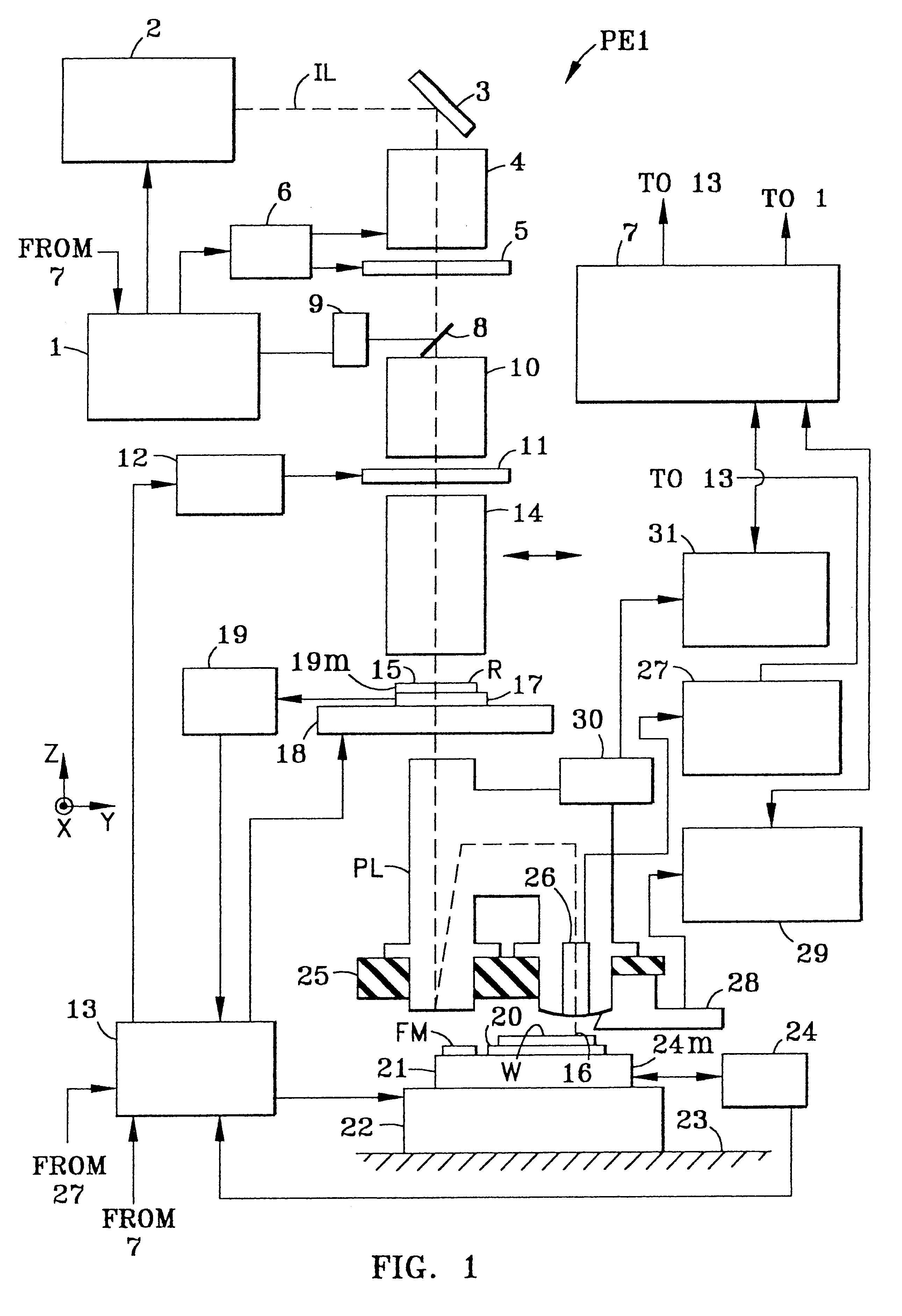
Satisfactory stability over time is thus obtained for the optical performance of the projection optical system.
Thus, the reduction in illumination efficiency is slight, since the absorptance with respect to illumination light beam IL for exposure is low.
However, nitrogen gas requires the replacement of a nitrogen gas cylinder when used continuously, and also requires partial replacement with air during exposure and during maintenance.

Method used


Image

  • Exposure apparatus and method
  • Exposure apparatus and method
  • Exposure apparatus and method

Examples


working example 1

FIG. 5 is a schematic optical diagram of the projection optical system according to Working Example 1. Projection optical system PL1 of Working Example 1 is optimized for an exposure energy beam having wavelength .lambda.=193.40 nm and a wavelength width (FWHM) of .+-.0.01 nm (.+-.10 pm).

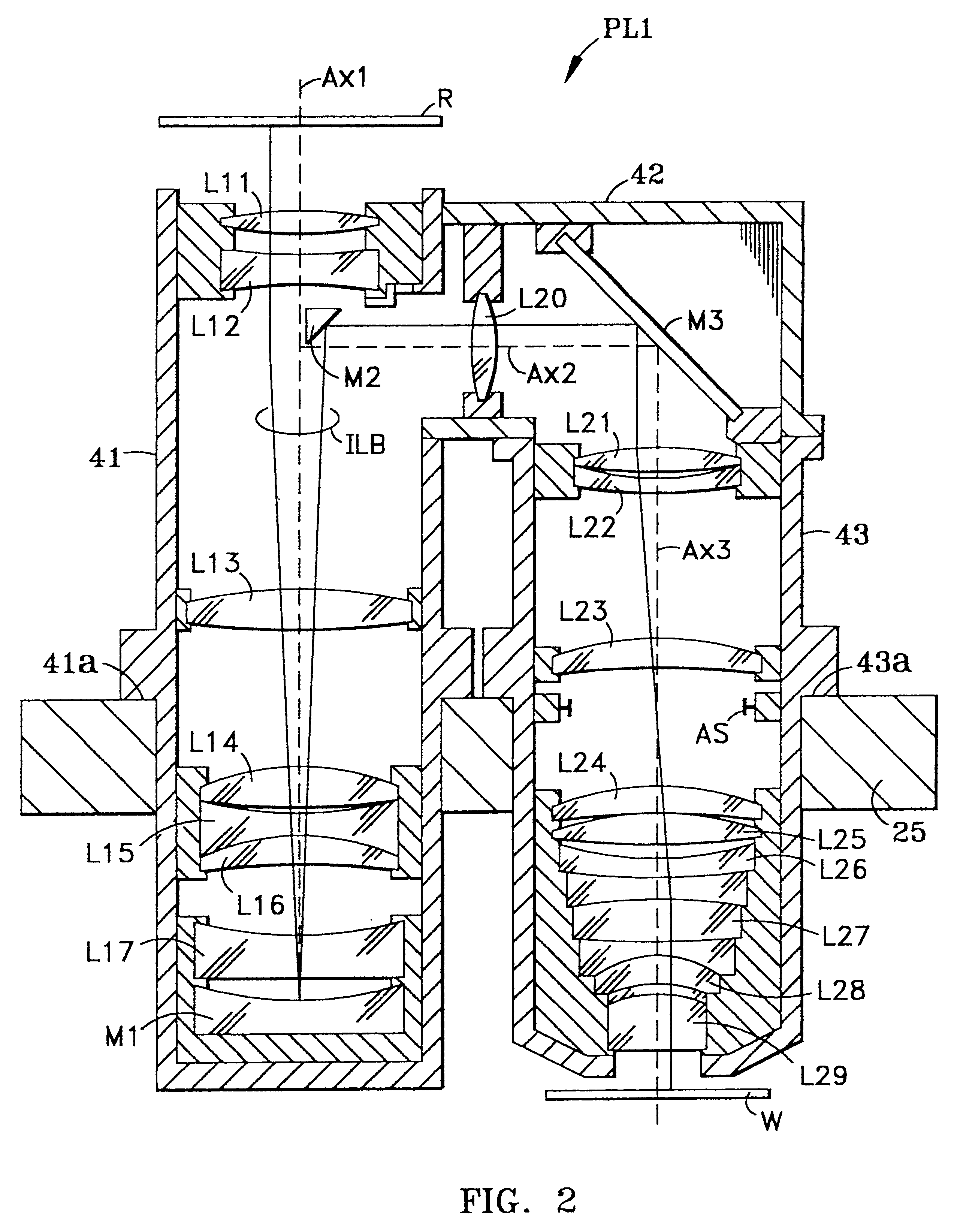
With reference to FIG. 5, projection optical system PL1 is provided with a first imaging system PLa that includes concave mirror M1 and that forms an intermediate image of reticle R, a second imaging system PLb that reimages this intermediate image onto wafer W with a predetermined reduction magnification, and folding mirror M2 arranged between first imaging system PLa and second imaging system PLb. Furthermore, although there is only one folding mirror in projection optical system PL1, a folding mirror may also be provided in second imaging system PLb, as shown in FIG. 2.

First imaging system PLa has first lens group G1 arranged most reticle-wise, second lens group G2 and concave mirror M1. Lens gro...

working example 2

FIG. 7 is a schematic optical diagram of a projection optical system PL2 according to Working Example 2. Projection optical system PL2 of Working Example 2 is optimized for an exposure energy beam having wavelength .lambda.=193.40 nm and a wavelength width (FWHM) of .+-.0.01 nm (.+-.10 pm).

Unlike the projection optical system PL1 according to Working Example 1 in FIG. 5, projection optical system PL2 does not form an intermediate image. Rather, projection optical system PL2 has a first lens group G1 with positive refractive power, beam splitter BS, second lens group G2 that includes concave mirror M1, and third lens group G3 having positive refractive power. Projection optical system PL2 does not have a folding mirror. However, a folding mirror may be provided in first lens group G1 to make the arrangement of reticle R and wafer W parallel. In addition, either a half mirror (half prism) that divides the amplitude or a polarizing beam splitter that separates polarized light can be us...

working example 3

FIG. 9 is a schematic optical diagram of a projection optical system PL3 according to Working Example 3. Projection optical system PL3 is optimized for an exposure energy beam having wavelength .lambda.=193.40 nm and a wavelength width (FWHM) of .+-.0.01 nm (.+-.10 pm).

In FIG. 9, projection optical system PL3 is provided with first imaging system PLa, second imaging system PLb, and folding mirror M2, the same as Working Example 1. Furthermore, a folding mirror may also be provided in second imaging system PLb.

As in Working Example 1, first imaging system PLa according to Working Example 3 has first lens group G1 arranged most on the reticle R side, and second lens group G2 and concave mirror M1. Lens groups G1 and G2 and the concave mirror are positioned so that the exposure energy beam that travels from the illumination optical system via reticle R passes sequentially through first lens group G1 and second lens group G2 and reaches concave mirror M1, and so that the exposure energy...


PUM

PropertyMeasurementUnit
wavelengthaaaaaaaaaa
full width at half maximumaaaaaaaaaa

Abstract

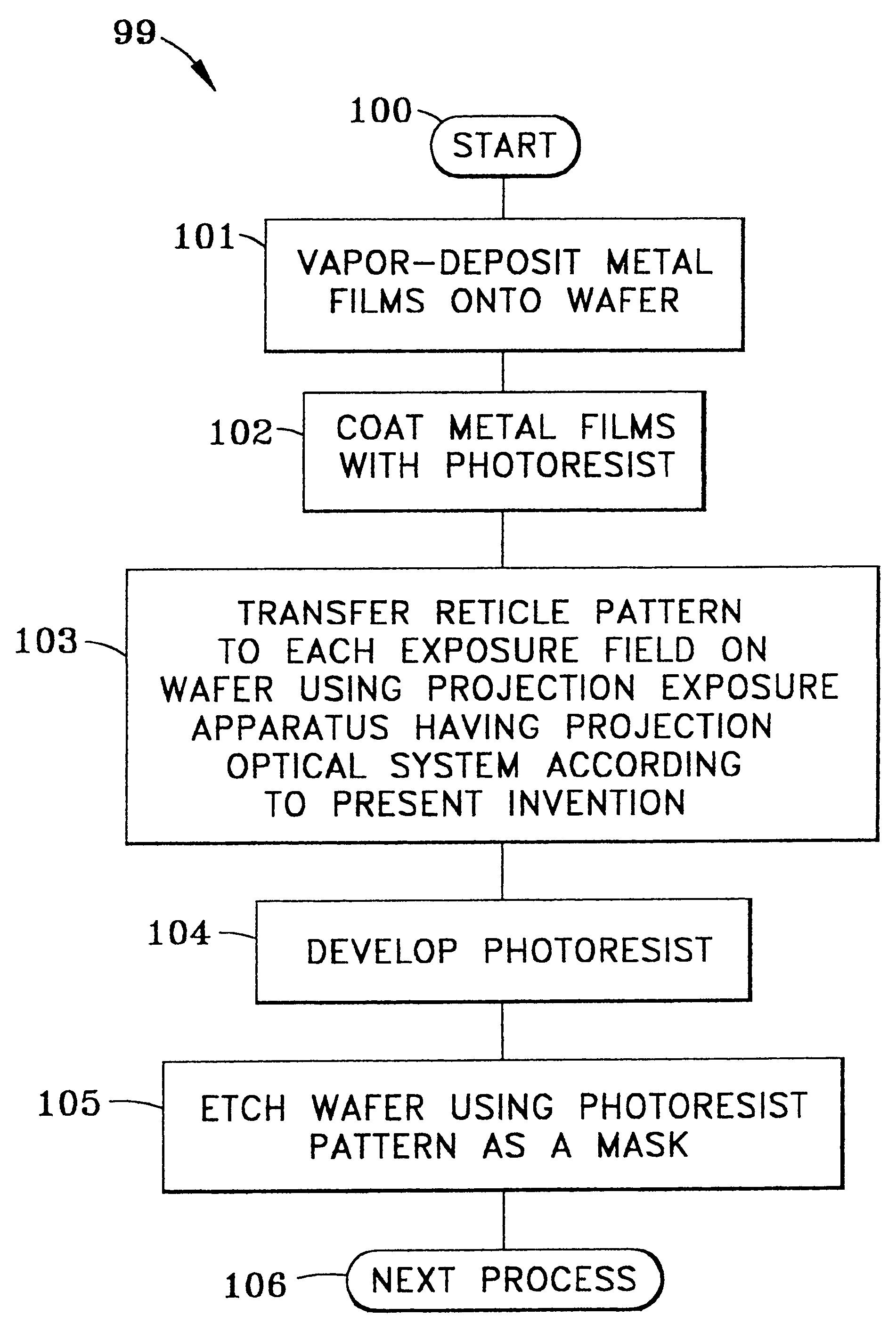
An exposure apparatus (PE1) and exposure method for use in photolithographically manufacturing devices such as semiconductor devices, image pickup devices, liquid crystal display devices and thin film magnetic heads. The apparatus is capable of transferring onto a substrate (W) the image of a pattern on a reticle (R) and includes a light source (2) capable of supplying an exposure energy beam (IL) with a wavelength under 200 nm, and an illumination optical system arranged to receive the exposure energy beam from said light source. The illumination optical system is designed to guide the exposure energy beam to the reticle. The apparatus also includes a projection optical system (PL) arranged between the reticle and the substrate. The projection optical system is capable of forming an image of the reticle pattern onto the substrate based on the exposure energy beam passing through the reticle. The projection optical system has a plurality of refractive optical members, wherein at least two such refractive optical members are arranged along an optical path of said exposure energy beam, and wherein each refractive optical member is made of at least two types of fluoride crystalline materials.

Description

The present invention relates to an exposure apparatus and exposure method, and in particular those used in photolithography for manufacturing devices such as semiconductor devices, image pickup devices, liquid crystal display devices and thin film magnetic headsBACKGROUND OF THE RELATED ARTWhen manufacturing semiconductor devices and the like, either a static exposure-type (e.g., stepper) or a scanning exposure-type (e.g., step-and-scan system) projection exposure apparatus is used to transfer the image of the pattern of a reticle as a mask onto a wafer (or glass plate and the like) coated with resist, via a projection optical system. With the advance of finer patterns in semiconductor integrated circuits and the like, it is desirable to improve the resolving power of the projection optical system provided in such exposure apparatus. This can be accomplished by shortening the exposure wavelength or increasing the numerical aperture (N.A.)The g-line (436 nm wavelength) to the i-line...

Claims


Application Information

Patent Timeline
Patent Type & Authority Patents(United States)
IPC IPC(8): G03F7/20
CPCG03F7/70058G03F7/70241
Inventor SUENAGA, YUTAKAOMURA, YASUHIRO
Owner NIKON CORP
Learn More