Process for producing an isolated planar high speed pin photodiode with improved capacitance

a high-speed pin and photodiode technology, applied in the field of improved, can solve the problems of reducing the yield rate affecting the efficiency of the pin photodiode, and the general practicability of thin wafers over this limit, so as to prevent the generation of slowly diffusing carriers and improve the dielectric isolation of the backside.

Inactive Publication Date: 2002-10-01
SILICON LAB INC
View PDF24 Cites 67 Cited by
  • Summary
  • Abstract
  • Description
  • Claims
  • Application Information

AI Technical Summary

Benefits of technology

The present invention describes several improved methods utilizing standard IC processing technology, V-groove or trench etching technology, lapping technology, combined with the novel use of a handling wafer to produce a PIN diode featuring 1) an arbitrarily thin intrinsic region which can be depl...

Problems solved by technology

Although a PIN photodiode outperforms a standard PN diode, it cannot be easily manufactured by standard semiconductor processes wherein fabrication is typically performed on only one side of the semiconductor wafer 12.
However, it is generally not practical to thin wafers beyond this limit without an excessive level of wafer breakage along with severe wafer handling and processing problems.
Consequently, the use of such a PIN photodiode in a high speed data receiver operating from a standard power supply voltage level of 2.7V-5V results in degraded speed performance.
Another problem with the structure of PIN diode 10 is that the connection of reflec...

Method used


Image

  • Process for producing an isolated planar high speed pin photodiode with improved capacitance
  • Process for producing an isolated planar high speed pin photodiode with improved capacitance
  • Process for producing an isolated planar high speed pin photodiode with improved capacitance

Examples


Embodiment Construction

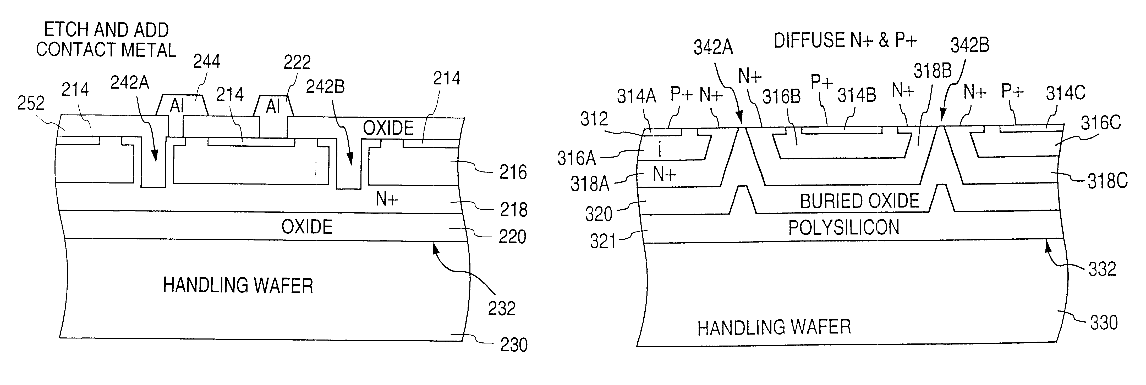
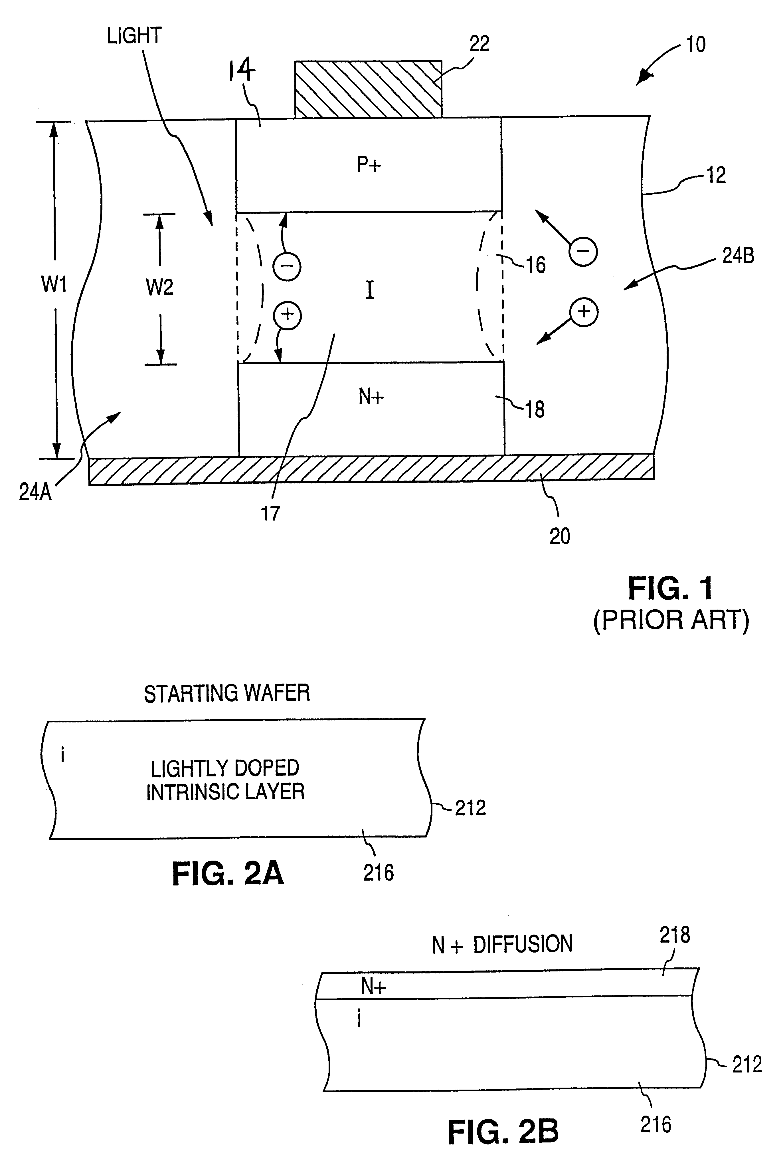
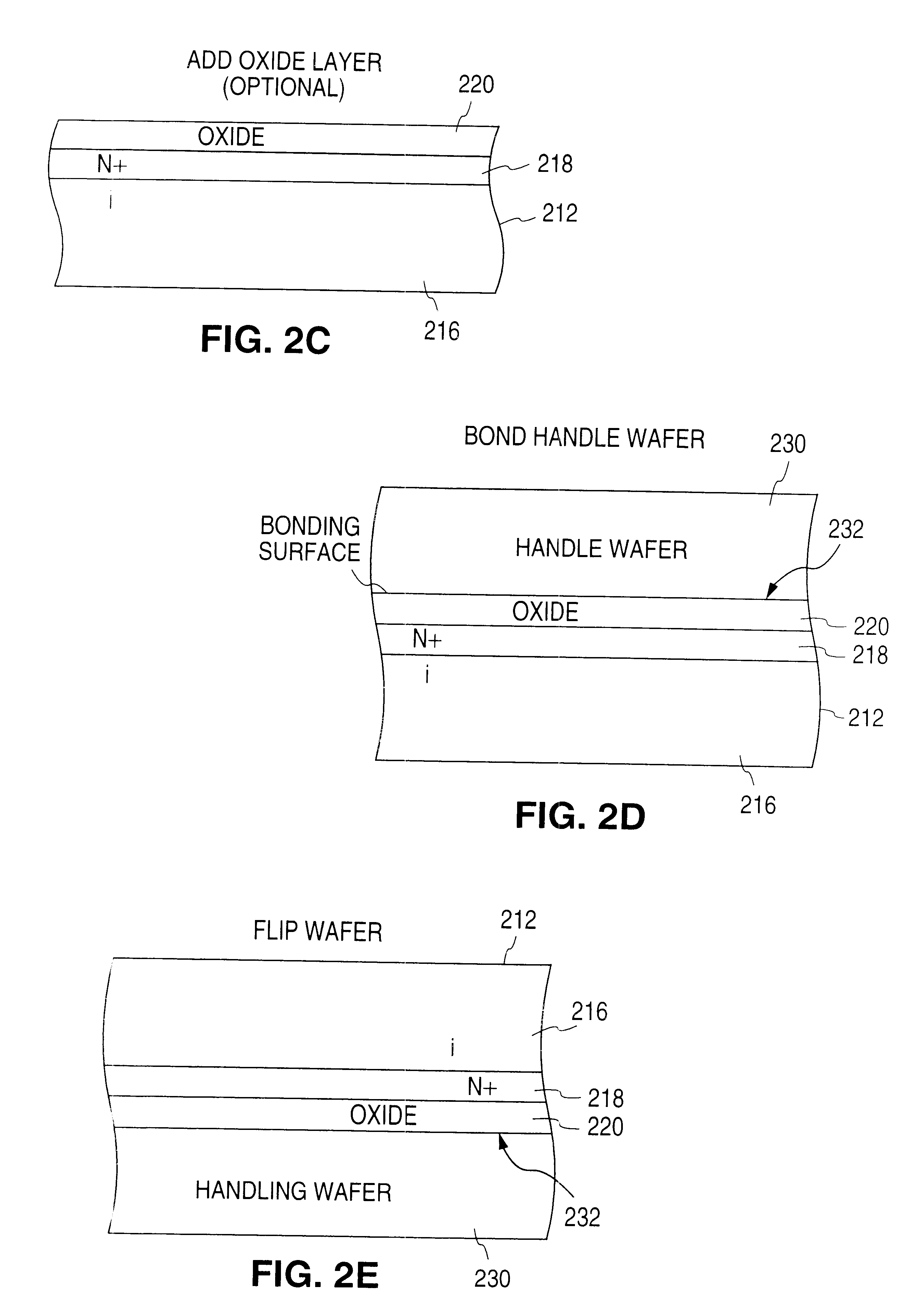
FIGS. 2A-L describe an improved PIN photodiode fabrication method which utilizes a standard thickness handling wafer with an isolating oxide layer grown on its surface that is bonded to the N.sup.+ diffusion side of a fabrication wafer. The handling wafer allows the intrinsic region of the fabrication wafer to be lapped to a thin thickness, as required for optimum performance of the PIN photodiode, while the handling wafer provides mechanical rigidity needed for processing. N.sup.+ and P.sup.+ regions are then diffused into the fabrication wafer. Next, diode trenches are etched around the periphery of each photodiode down to the N+ region. The sidewalls of the trenches are then N+ diffused before being covered with an oxide layer and then filled with polysilicon. Finally, coplanar metal contacts to the N+ and P+ regions are formed.

The process begins with fabrication wafer 212 of FIG. 2A, which is lightly N doped to form an intrinsic layer 216 which will later become the intrinsic re...


PUM


Abstract

A method is shown for producing a PIN photodiode having low parasitic capacitance and wherein an intrinsic layer of the photodiode can be made arbitrarily thin. A fabrication substrate is lightly doped to have a first conductivity type in order to form the intrinsic layer of the photodiode. A first active region of the photodiode having the first conductivity type is formed on a first surface of the fabrication substrate. An oxide layer is also formed upon the first surface of the fabrication substrate. A first glass layer is formed on a first surface of a handling substrate. The first surface of the handling substrate is bonded to the first surface of the fabrication substrate. A second surface of the fabrication substrate is then lapped to a obtain a preselected thickness of the intrinsic layer. A second active region of the photodiode having a second conductivity type is formed on the second surface of the fabrication substrate. A groove is etched from the second surface of the fabrication substrate through the intrinsic region to the first surface in order to isolate the photodiode. A second glass layer may be formed on a second surface of the handling substrate to further reduce parasitic capacitance.

Description

1. Field of the InventionThe present invention is directed toward an improved manufacturing process for a producing an isolated planar high speed PIN photodiode.2. Description of the Related ArtPhotodiodes are diodes in which charge carriers are generated responsive to light incident upon the photodiode. Any PN junction diode which admits light can function as a photodiode. A photodiode outputs voltage or current when absorbing light. In a photodiode which is intended for high speed communication systems, it is important to optimize the performance for light conversion efficiency, speed (minimal transit time delay), minimum RC time constant, ability to operate at low reverse bias voltage, and cost in the application in which the photodiode will be employed.FIG. 1 illustrates the structure of a conventional PIN photodiode 10. A wafer 12 is lightly doped with N dopant in order to produce an intrinsic region 16. A P+ region 14 is formed on one surface of the wafer and an N+ region 18 i...

Claims


Application Information

Patent Timeline
IPC IPC(8): H01L31/0352H01L31/102H01L31/0248H01L31/105
CPCH01L31/0352H01L31/035281H01L31/105Y02E10/50
Inventor IRISSOU, PIERRE
Owner SILICON LAB INC
Why Eureka
Try Eureka