Although the underlying technology for this process appears fairly simple and direct, there are many complications in the actual performance of the process.
These are high performance standards that are not readily achieved,
For this reason, this method is inappropriate for forming a micropattern such as a gate
electrode.
However, the metal film formed by this method was formed by CVD (
Chemical Vapor Deposition) at a low temperature because of a resist film.
For this reason, bonding between a metal multilayer and a
semiconductor substrate constituting an
electrode pattern was inadequate.
However, each such different
system requires fundamental investigation of the properties and the
processing necessities.
A significant manufacturing problem in every form of printed circuit manufacture is the assurance of appropriate registration of the circuitry, and especially the connect points, in the layers of circuits that are combined.
For example, even in stacking circuits by etching layers in place, there can be significant registration problems.
If the contact points are not aligned vertically through the stacked array of circuits in the circuit board, the electrical connectors passing through the layers may not make the required contact with the circuit elements and the circuit board will be partially non-functional.
For example, in forming the stacked arrays by stacking circuits and by etching layers in place, registration can be compromised by a) temperature changes occurring during
processing causing layers to thermally expand and then contract, distorting the circuit image, b) physical mislaying of layers on top of each other, c) misalignment of the stack within the
exposure area of a
photoresist imaging systems, d) vibration shifting either the circuit element or the imaging element (e.g., the
laser diode for the imaging of the resist), and the like.
In the development of new systems and processes for the manufacture of circuit boards, the nature of registration problems must be addressed early in the development cycle or severe problems will be encountered during scale-up.
Another likely cause of misregistration e) is a
volume change in adhesives during curing or setting.
This is difficult enough where only two (e.g., tri-metal) sub-elements are connected on opposite sides of a support, but the difficulty is magnified with more layers or when sheets of (preferably tri-metal) material are used from rolls or coils, and the lamination of the (e.g., etched tri-metal) sub-elements occurs in a continuous fashion.
In the last process, misregistration can readily
creep and increase in the layers as they are laminated due to the multiplying effect of slightly misregistered panels or circuits in coil or roll form.
Rather than losing a single circuit board in that circumstance, an entire run of circuit boards could be lost.
The etching of details into metal layers can be a complex and difficult task.
The complexity and difficulty varies greatly between emtal layer systems depending upon the number of metal layers, the types of metal layers, the resolution required in the etching process, and other aspects of the materials and constructions used.
If the change in relative position between the two layers creates an
internal stress (e.g., when an elastically stressed or stretched layer is laminated to an unstressed or unstretched layer), release of the externally applied tension after the layers have been laminated or otherwise joined will leave the stress between the layers within the finished article, and there could be a shearing stress within the article of sufficient strength to damage elements of the circuitry, particularly smaller, fragile elements of the circuitry, such as air bridges, or create alignment issues.
The manufacture of circuit boards has become a highly competitive field, with circuit boards being needed in essentially all modren electrical appliances and games, yet with their individual design having to be tailored for each field of use, their production having to be rapid and cost efficient, the volume capacity being extremely large, and the requirements for quality being absolute since failure of the circuitry will render each product useless.
This could prove difficult, however, as most commercial photoresists are removed when exposed to etchants that have a pH in excess of 10.5, that are used to etch the aluminum layer.
Uneven aluminum thickness or non-uniform etching of the
copper or
aluminum can result in undesired aluminum features remaining, which could result in electrical shorts.
Failure to control etch temperature can damage both the circuit being etched and the equipment which contains the etchant.
Some of the oxidizers that enhance the performance of the high pH etch
system, for example
sodium nitrate and especially
sodium bromate, are both expensive and environmentally unfriendly.
Although by controlling the flow rate of the curable
polymer system under the bridge, some stress forces can be reduced, this might require extremely slow production rates for higher molecular weight / higher
viscosity compositions, and is not preferred.
1) Flowing under and over air bridges without bending or breaking them
3) Protecting the underlying circuit from
corrosion, abrasion, vibration and physical damage
4) Producing multi-layer ETM on an inline coil process gives process economy, but introduces a difficult problem of precision alignment of 3 moving coils. We describe a system including accumulators and coil
grippers or sprockets, which permit the precision positioning of the 3 layers with no
relative motion. It is then possible to join them in a nip, hot roll lamination process.
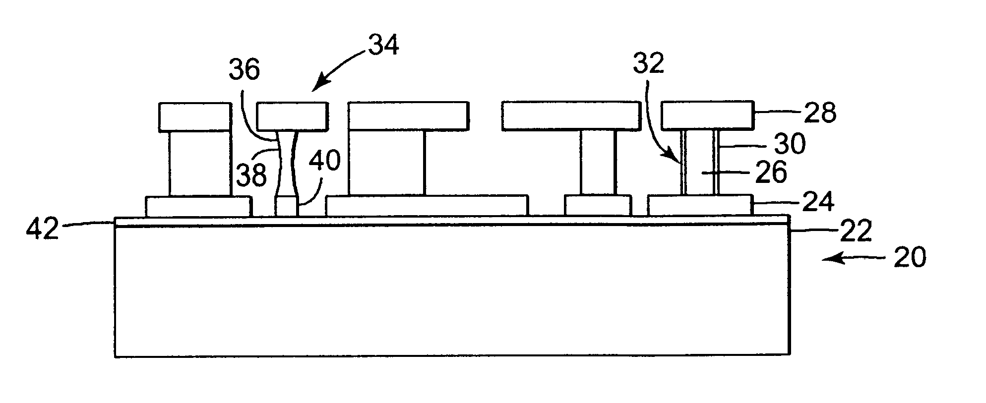
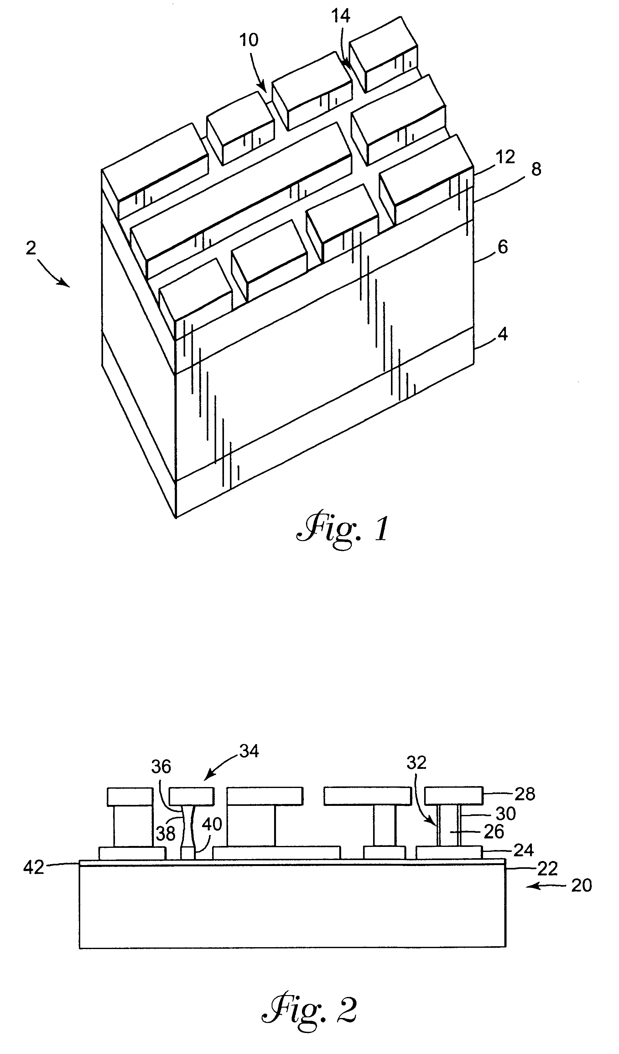
The etched tri-metal circuit may be relatively fragile, depending upon the thickness of the various elements and layers, the dimensions of the circuit elements themselves, and the amount of additional structural support provided for the elements (e.g., the polymeric support for air bridges described above).
The etching of the central aluminum core layer from a Cu / Al / Cu structure can result in oxidation of the
copper circuits, which may or may not have to be cleaned away.
The precision alignment and superposition of material from 3 separate, moving coils is difficult.
The peroxy-sulfuric system, which etches
copper in the presence of aluminum, gives a poor profile.
Failure of a current would indicate lack of alignment.

