Gallium phosphide luminescent device

a luminescent device and gallium phosphide technology, applied in the direction of semiconductor/solid-state device manufacturing, semiconductor devices, electrical apparatus, etc., can solve the problems of difficult to control the carrier concentration independently from the n concentration, difficult to further raise the luminance at a stable wavelength, and disadvantageous in terms of obtaining pure green light emission

Inactive Publication Date: 2002-11-12
SHIN-ETSU HANDOTAI CO LTD
View PDF6 Cites 6 Cited by
  • Summary
  • Abstract
  • Description
  • Claims
  • Application Information

AI Technical Summary

Problems solved by technology

Raising the N concentration, however, cause red-shift of the dominant emission wavelength to intensify yellow component, so that it has been difficult to further raise luminance at a stable wavelength.
In addition, while the ammonia gas introduction during the growth of the n-type GaP layer 43 inevitably reduces the Si (donor) concentration, to thereby advantageously raise the injection efficiency of holes responsible for the light emission, this will raise another problem in that the donor concentration of the n-type GaP layer 43 will always vary in

Method used


Image

  • Gallium phosphide luminescent device
  • Gallium phosphide luminescent device
  • Gallium phosphide luminescent device

Examples


first embodiment

(First Embodiment)

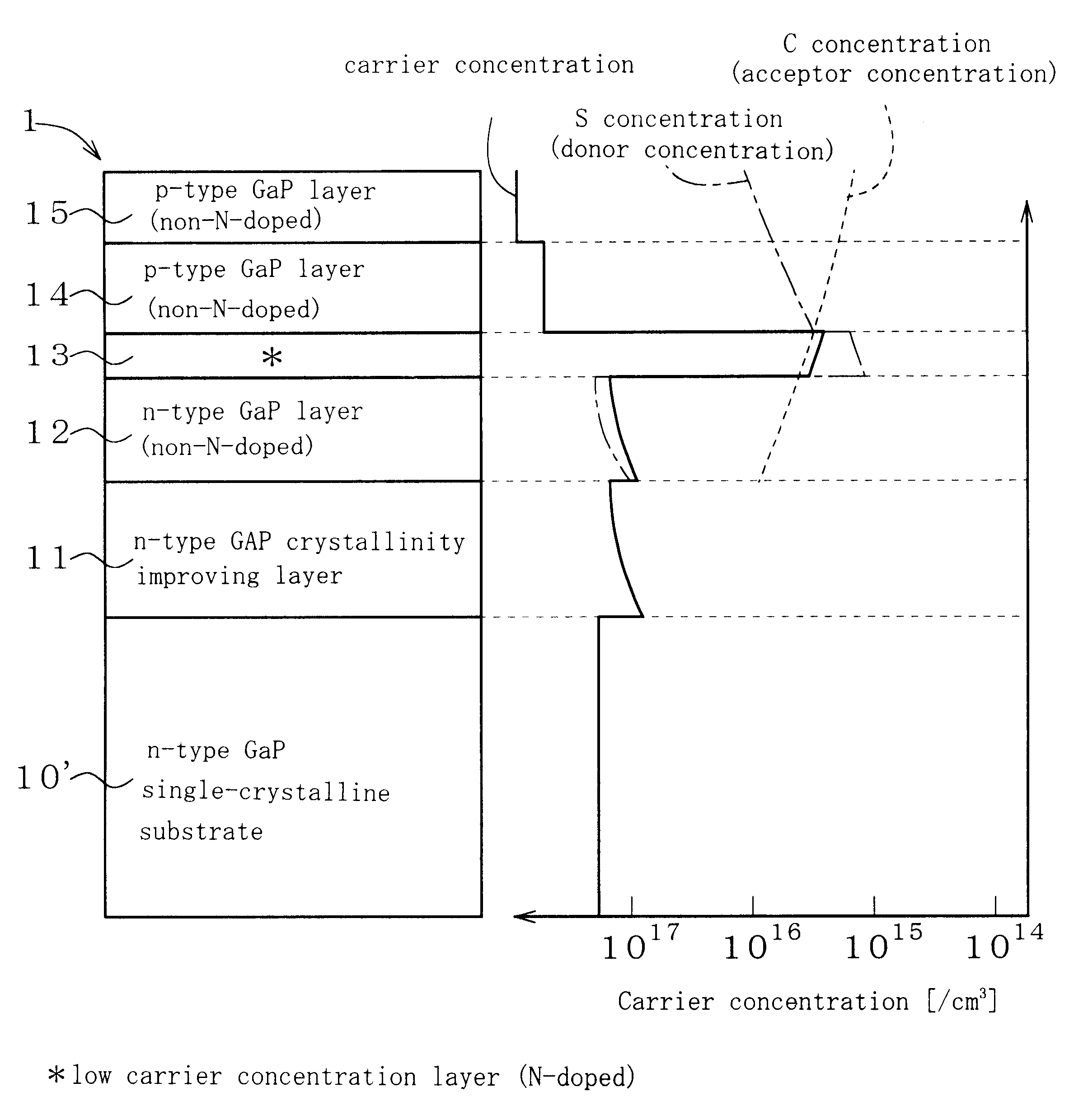
FIGS. 1A and 1B are schematic drawings respectively showing a section and depth profile of the carrier concentration of a GaP light emitting device according to the present invention. For simplicity, FIG. 1A does not show electrodes provided on the "n" terminal and "p" a terminal surfaces.

As shown in FIG. 1A, the GaP light emitting device 1 of the present invention has on an n-type GaP single-crystalline substrate 10, an n-type GaP crystallinity improving layer 11, an n-type GaP layer 12, a low carrier concentration layer 13, and p-type GaP layers 14 and 15 stacked in this order. The n-type GaP single-crystalline substrate 10 and the n-type GaP crystallinity improving layer 11 are added with silicon (Si) as an n-type dopant. On the other hand, the n-type GaP layer 12 is added with sulfur (S) and carbon (C) as impurities (note that the n-type GaP layer 12 in this embodiment is not doped with N).

The low carrier concentration layer 13 is a p-type GaP layer in this emb...

second embodiment

(Second Embodiment)

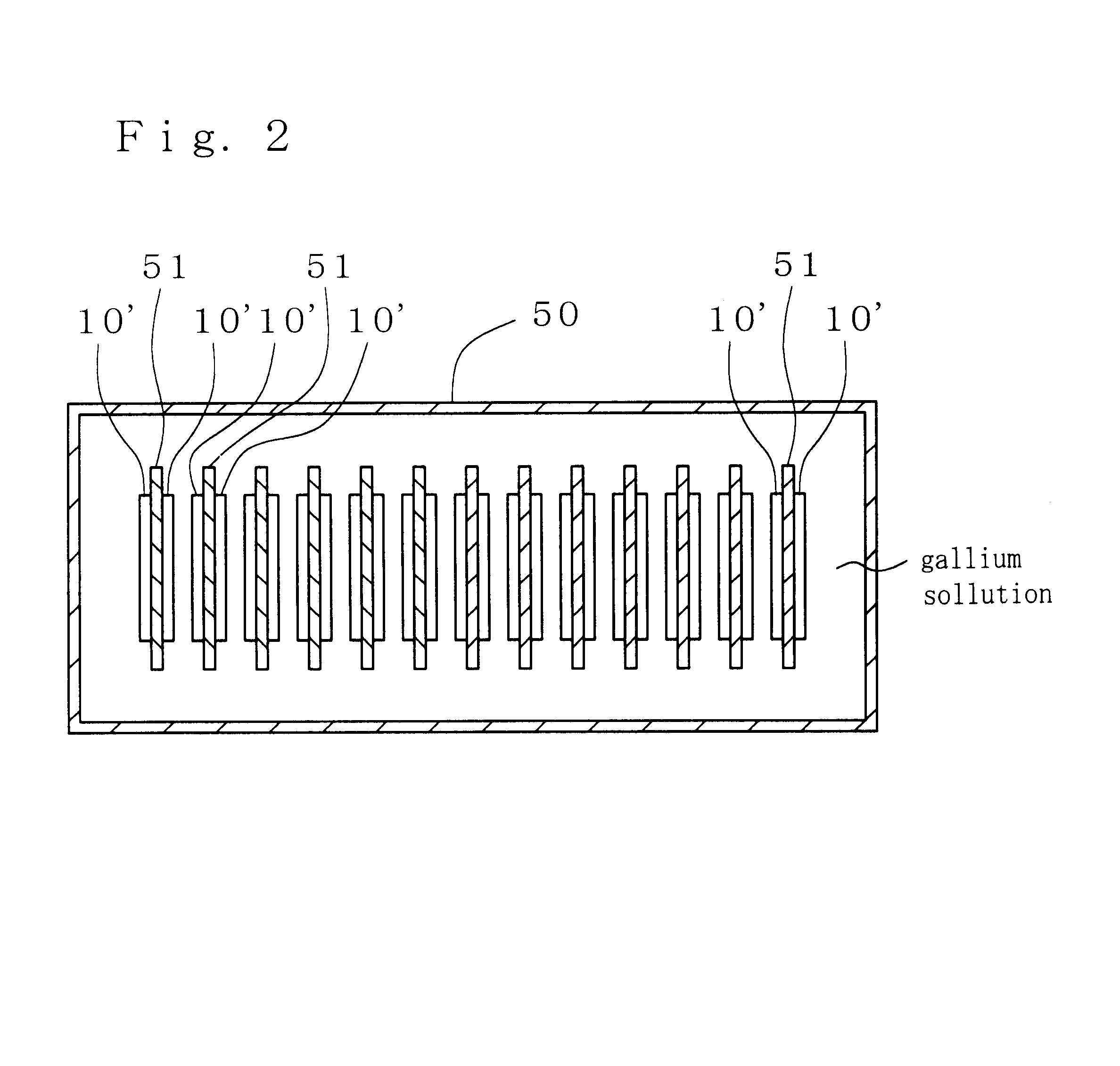
An exemplary method for fabricating the GaP light emitting device 1 shown in FIG. 1A will be described. FIG. 6 shows a typical constitution of a liquid-phase epitaxial growth apparatus used for growing, by the liquid-epitaxial growth method, the individual layers on the GaP single-crystalline substrate 10'. As shown in FIG. 6, in a process tube 23, a carbon-made slide boat 24 (growth vessel) having a wafer chamber 25 for housing a compound semiconductor wafer 30 (the n-type GaP single-crystalline substrate 10' having an epitaxially grown layer formed thereon) is set, and a bottom-opened solution reservoir 27 containing a gallium solution 28 is provided thereon so that it can slide on the slide boat 24 with the aid of a sliding rod 26 (that is, so that the slide boat 24 can slide relative to the gallium solution 28). The gallium solution 28 is dissolved with S as an n-type dopant.

In the process tube 23 and on the side of a carrier gas supply port 31, Zn 29 as a p-t...

third embodiment

(Third Embodiment)

In this embodiment, another method for fabricating the GaP light emitting device 1 shown in FIG. 1A will be described referring to process diagrams shown in FIGS. 8A to 8H. First, as shown in FIG. 8A, the gallium solution 16 obtained by dissolving at 1060.degree. C. polycrystalline GaP and Si as an n-type dopant is placed on the n-type GaP single-crystalline substrate 10'. The temperature of a system including the gallium solution 16 is gradually lowered, to thereby allow GaP dissolved in the gallium solution 16 to deposit onto the n-type GaP single-crystalline substrate 10'. Thus the compound semiconductor wafer 30 composed of the n-type GaP single-crystalline substrate 10' and the Si-doped n-type GaP crystallinity improving layer 11 formed thereon is obtained (FIG. 8B).

Next, as shown in FIG. 8C, a gallium solution 17 containing S as an n-type dopant dissolved therein at a concentration higher than that in a gallium solution 18 described later is placed on the com...


PUM


Abstract

By providing a nitrogen-doped low carrier concentration layer 13 having both of a donor concentration and an acceptor concentration controlled below 1x10¹⁶/cm3 at a p-n junction portion between an n-type GaP layer 12 and a p-type GaP layer 14, the luminance of the GaP light emitting device can be improved by as much as 20 to 30% over the conventional one. Suppressing the donor concentration and the acceptor concentration in the low carrier concentration layer 13 below 1x10¹⁶/cm3 inevitably gives a carrier concentration, which is expressed as a difference between both concentrations, lower than 1x10¹⁶/cm3 accordingly. The emission efficiency upon injection of electrons or holes can be improved by suppressing the concentration of the donor which serves as non-emissive center below 1x10¹⁶/cm3 to thereby extend the carrier lifetime; and by concomitantly suppressing the carrier concentration at a level significantly lower than that in the adjacent layers 12 and 14.

Description

The present invention relates to a gallium phosphide light emitting device and a method for fabricating thereof, and in more detail, a gallium phosphide light emitting device with a high luminance and a method for fabricating such device.DESCRIPTION OF THE BACKGROUND ARTLight emitting devices such as light emitting diodes are generally obtained by stacking a plurality of semiconductor layers on a semiconductor substrate to thereby fabricate a multi-layered semiconductor wafer having a p-n junction, and processing such wafer into the devices. Among such devices, those having a dominant emission wavelength (dominant wavelength) within a range from 555 to 580 nm are obtained by stacking on an n-type gallium phosphide (which may simply be noted as "GaP" hereinafter) substrate at least one each of n-type and p-type gallium phosphide layers in this order, and processing the obtained wafer into the devices. A method for determining the dominant emission wavelength (dominant wavelength) is ...

Claims


Application Information

Patent Timeline
IPC IPC(8): H01L33/00H01L33/30
CPCH01L33/025H01L33/30Y10S438/918
Inventor YAMADA, MASATOHIGUCHI, SUSUMUYUMOTO, KOUSEIKAWASAKI, MAKOTOAIHARA, KEN
Owner SHIN-ETSU HANDOTAI CO LTD
Why Eureka
Try Eureka