Laser irradiation method, laser irradiation apparatus, and semiconductor device

a laser irradiation and laser technology, applied in the field of semiconductors, can solve the problems of poor crystallinity of a semiconductor film irradiated with this region, insufficient crystallinity, and drawbacks where these stipes appear on the screen

Inactive Publication Date: 2003-03-18
SEMICON ENERGY LAB CO LTD
View PDF35 Cites 141 Cited by
  • Summary
  • Abstract
  • Description
  • Claims
  • Application Information

AI Technical Summary

Problems solved by technology

The semiconductor characteristics of the film differ remarkably for each of these stripes, so if this striped film is used when forming an integrated driver and pixel (system on panel) liquid crystal display device, a drawback develops where these stipes appear on the screen, as is.
This problem is being remedied by improving the film quality of the non-single crystal silicon film, the laser irradiation object, but this is not yet enough.
The crystallinity of a semiconductor film irradiated with this region is poor relative to a region exposed to the center of the beam.
If the silicon film is thicker than 50 nm, there is a tendency for the off characteristics to become poor, while a thinner film influences the reliability.

Method used


Image

  • Laser irradiation method, laser irradiation apparatus, and semiconductor device
  • Laser irradiation method, laser irradiation apparatus, and semiconductor device
  • Laser irradiation method, laser irradiation apparatus, and semiconductor device

Examples


embodiment 1

The calculation method of the relationship between the laser power and the maximum spot size, estimated in the above embodiment mode of the present invention, is shown here.

The amorphous silicon film formed on the above substrate is taken as a model. The thermal conductivities of the silicon oxide film and the amorphous silicon film are taken as 0.02 W / cm.multidot.K and 0.2 W / cm.multidot.K, respectively, from room temperature to 1200.degree. C. (the temperature assumed to be the melting point of the amorphous silicon film used throughout this specification). The thermal conductivity in the range beyond the melting point temperature of the amorphous silicon film is taken as 2 W / cm.multidot.K.

The temperature limitations of each of the films during laser crystallization of the amorphous silicon film are as below.

The glass substrate can be heated up to a maximum of 600.degree. C. without any change in shape (the distortion temperature of Corning 1737 is above 600.degree. C.). On the oth...

embodiment 2

The spot size calculated in embodiment 1 above is very small, so it is difficult to use for mass production. An example of increasing the laser beam size by a great jump through use of a high distortion point temperature quartz substrate as a substrate is shown, then, in embodiment 2. A quartz substrate does not change in shape, or in quality, at all when heated to the melting point of a silicon film. Therefore, the beam size can be made wider. The irradiation object in embodiment 2 is the substrate having a silicon film formed thereover shown in the embodiment mode of the present invention, where the glass substrate is replaced with a 1.1 mm thick quartz substrate.

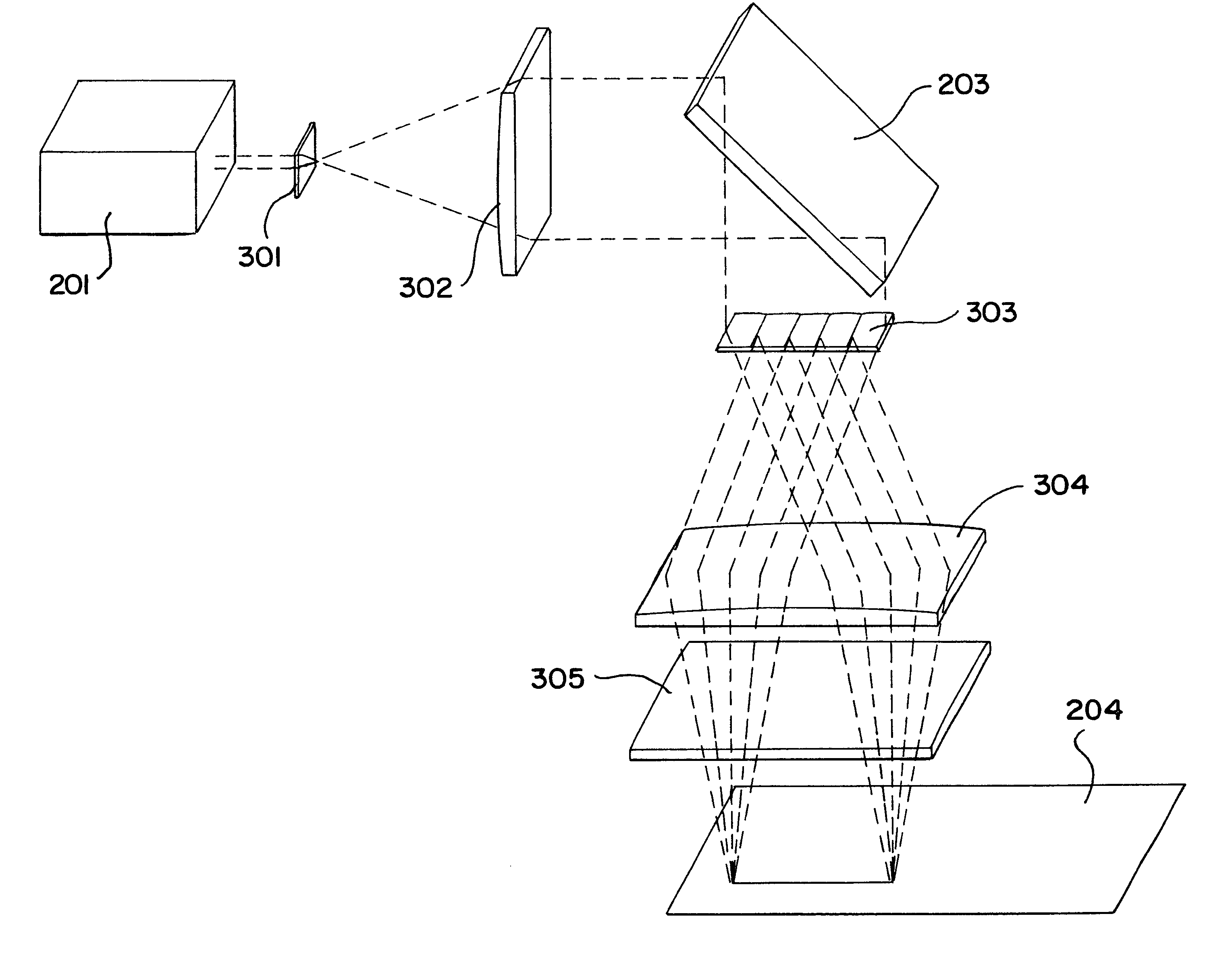
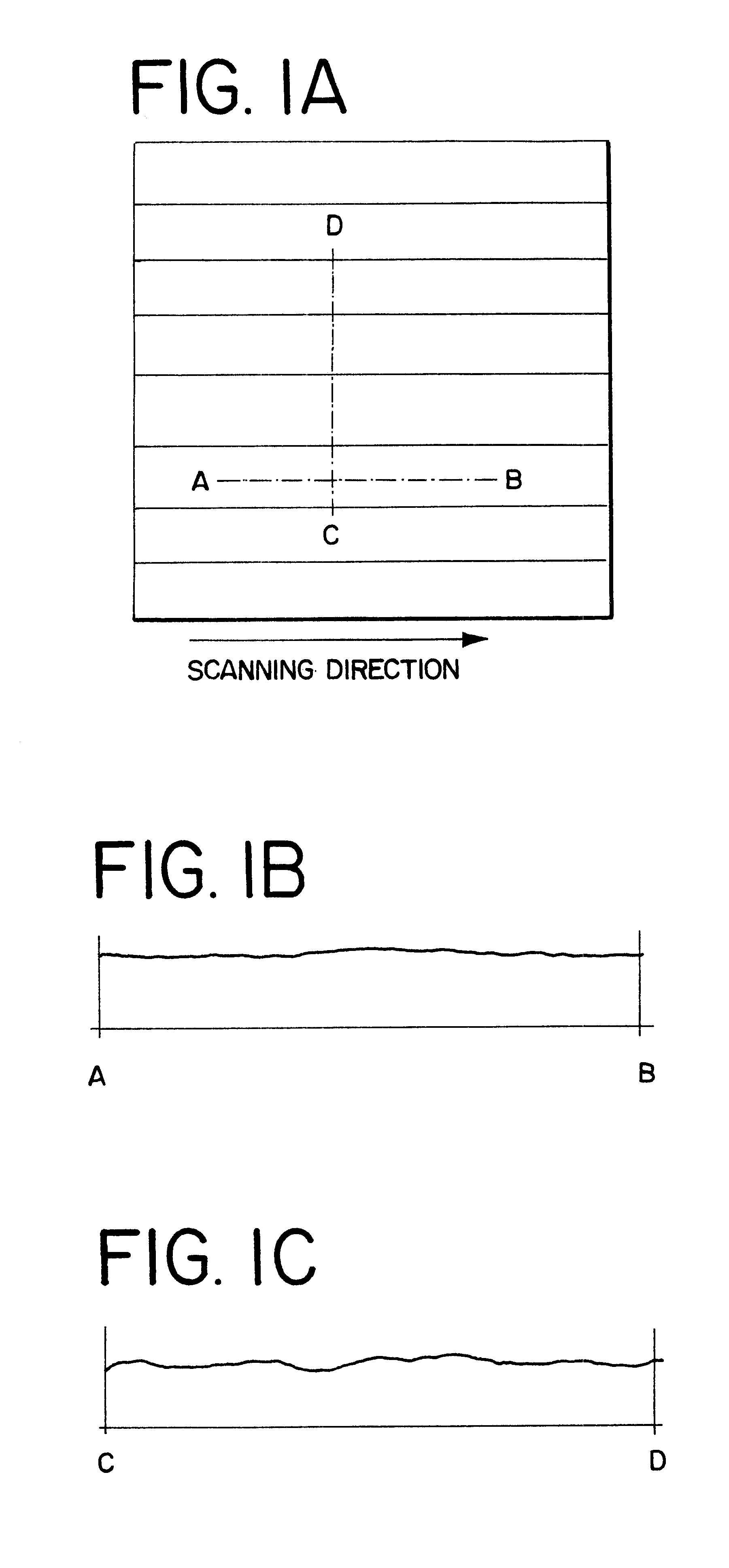
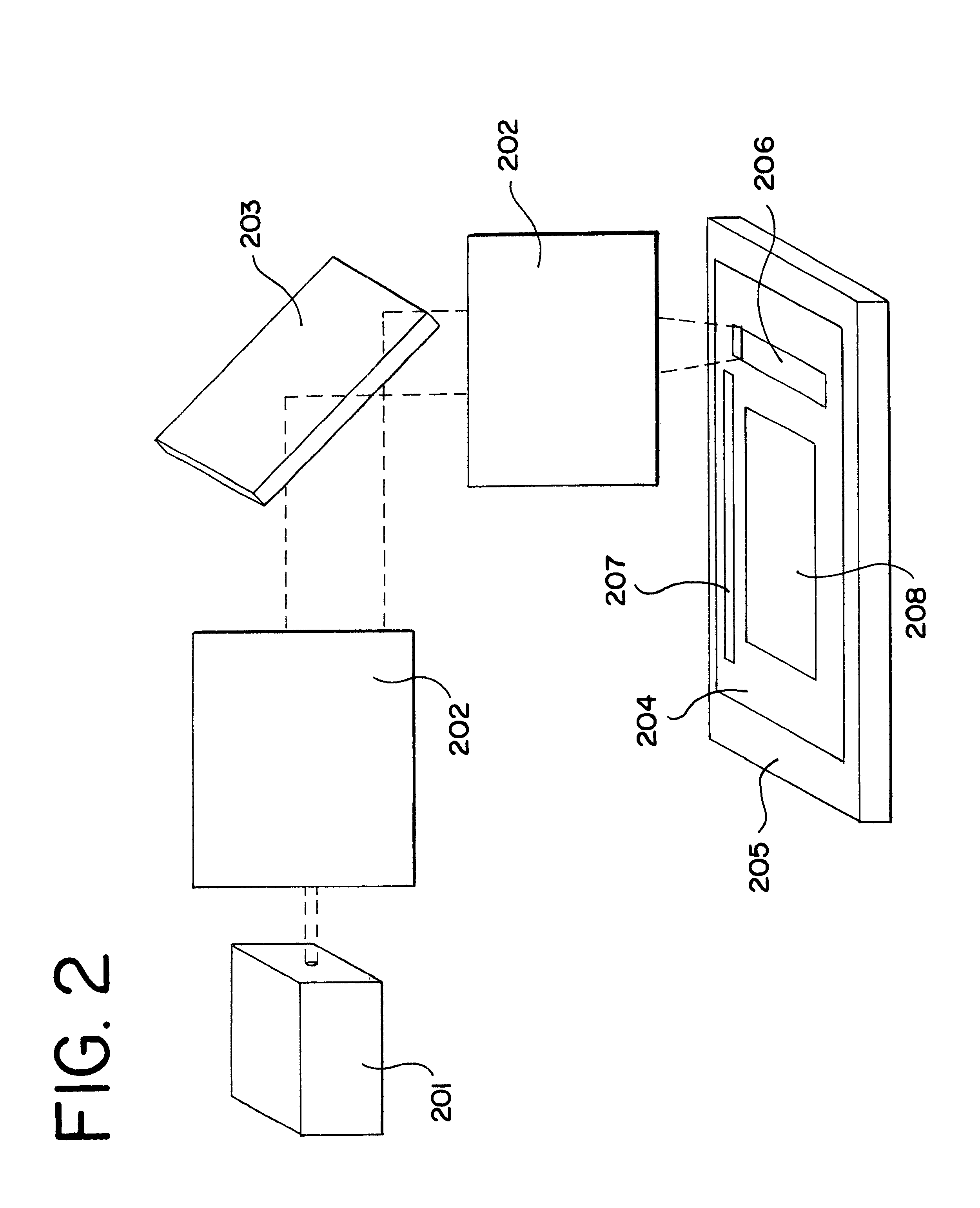
An example using a 1000 W continuous emission excimer laser processed into a linear beam shape (with a size of 125 mm .times.0.4 mm) is shown in embodiment 2. The means of processing the laser into a linear beam shape is shown in FIG. 8.

The device shown in FIG. 8 possesses a function of irradiating as a linear shape beam ...

embodiment 3

Embodiment 3 shows a process of crystallizing a silicon film formed on a glass substrate using a 1000 W continuous emission excimer laser with the same specifications as that of embodiment 2. An example is shown in which the extreme surface of the glass substrate melts by the crystallization process of embodiment 3, so a base film is made rather thick in order to prevent contamination of the silicon film.

First, a 125.times.125.times.0.7 mm glass substrate (Corning 1737) is prepared as a substrate. This substrate has sufficient durability up to a temperature of 600.degree. C. A 400 nm silicon oxide film is deposited on the glass substrate as a base film. In addition, a 55 nm thick amorphous silicon film is deposited on top. Sputtering is used for both film depositions. Alternately, film deposition may also be performed by plasma CVD. The substrate, on which the above films have been deposited, is then exposed to a hot bath at 450.degree. C. for 1 hour. This process is one for reducin...


PUM


Abstract

An object of the present invention is obtaining a semiconductor film with uniform characteristics by improving irradiation variations of the semiconductor film. The irradiation variations are generated due to scanning while irradiating with a linear laser beam of the pulse emission. At a laser crystallization step of irradiating a semiconductor film with a laser light, a continuous light emission excimer laser emission device is used as a laser light source. For example, in a method of fabricating an active matrix type liquid crystal display device, a continuous light emission excimer laser beam is irradiated to a semiconductor film, which is processed to be a linear shape, while scanning in a vertical direction to the linear direction. Therefore, more uniform crystallization can be performed because irradiation marks can be avoided by a conventional pulse laser.

Description

1. Field of the InventionThe present invention relates to a semiconductor device having a circuit structured with a thin film transistor. For example, it relates to the structure of an electro-optical device, typically a liquid crystal display device, and of an electric equipment loaded with such an electro-optical device as a component. Note that throughout this specification, the semiconductor device indicates general devices that may function by use of semiconductor characteristics, and that the above stated electro-optical device and electric equipment are categorized as the semiconductor device.2. Description of the Related ArtIn recent years, the technique of crystallizing and improving the crystallinity of an amorphous semiconductor film or a crystalline semiconductor film (a semiconductor film having crystallinity which is polycrystalline or microcrystalline, but is not a single crystal), in other words a non-single crystal semiconductor film, formed on an insulating substra...

Claims


Application Information

Patent Timeline
Patent Type & Authority Patents(United States)
IPC IPC(8): H01L21/20H01L21/02H01L27/12H01L21/70H01L21/84G02B27/09H01L21/77H01S3/13
CPCG02B19/0014G02B27/0961G02B27/0966G03F7/2053H01L21/02422H01L21/02488H01L21/02532H01L21/02672H01L21/02675H01L21/02686H01L21/02691H01L27/1277H01L27/1285H01L27/1296H01L29/78627G02B19/0052G02B27/0911G02B27/0955
Inventor YAMAZAKI, SHUNPEITANAKA, KOICHIRO
Owner SEMICON ENERGY LAB CO LTD
Why Eureka
Try Eureka