Analog to digital converter using subranging and interpolation
- Summary
- Abstract
- Description
- Claims
- Application Information
AI Technical Summary
Benefits of technology
Problems solved by technology
Method used
Image
Examples
Embodiment Construction
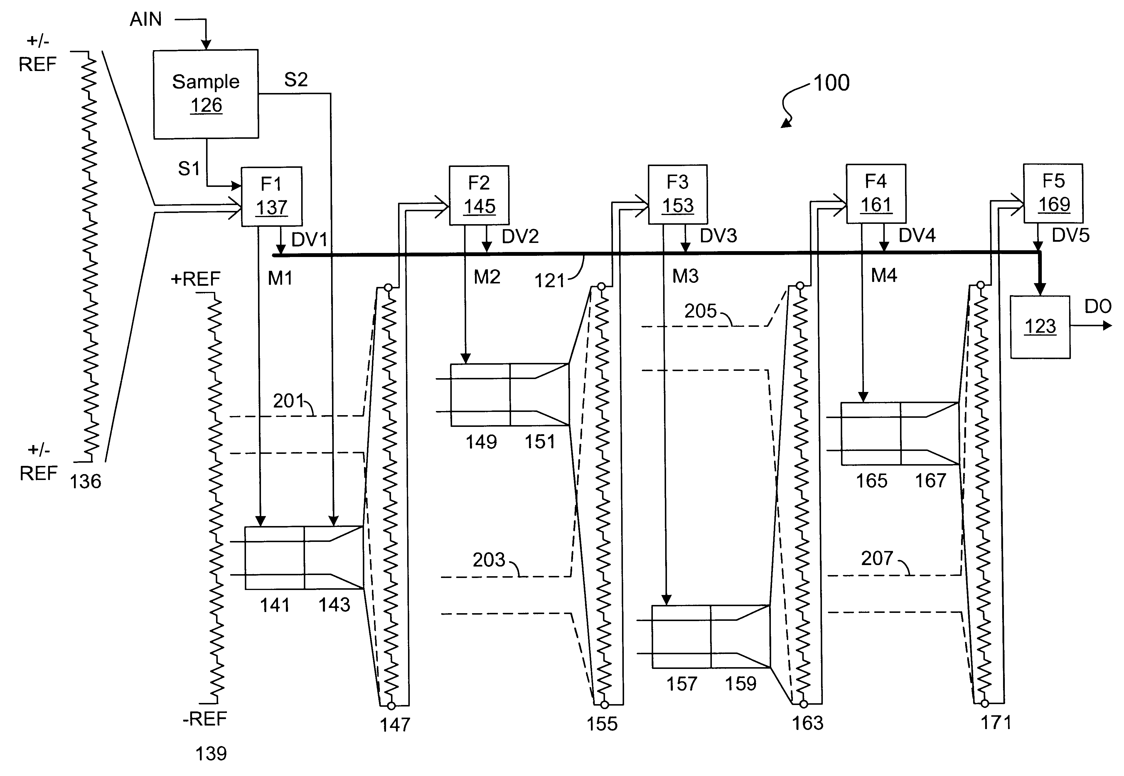
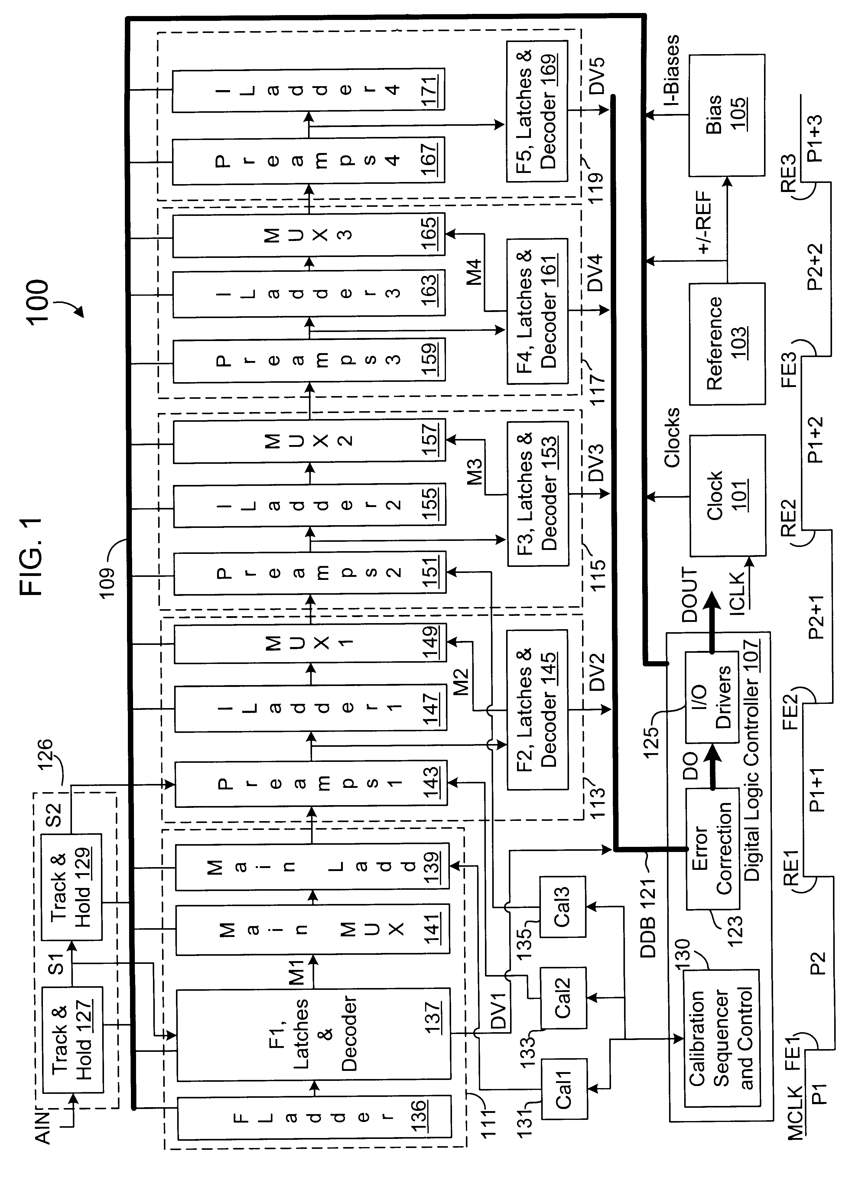
FIG. 1 is a block diagram of an exemplary 14-bit analog to digital converter (ADC) 100 in accordance with an embodiment of the present invention. The ADC 100 includes support circuitry, such as a clock circuit 101, a reference circuit 103, a bias circuit 105 and a digital logic controller 107, all coupled together via a bias / clock bus 109. The clock circuit 101 receives an input clock signal ICLK and generates a plurality of clock signals "Clocks" for providing synchronization of the various components of the ADC 100. The reference circuit 103 generates reference voltage signals +REF and -REF that are sufficiently independent of temperature and power supply variations. The + / -REF signals are provided to the bias circuit 105, which develops a plurality of temperature-independent bias current signals "I-Biases" that provide current biasing for various components of the ADC 100 including preamplifiers within pipelined stages, as further described below.
The signals of the bias / clock bus...
PUM
 Abstract
Description
Claims
Application Information


