Method of sputtering copper to fill trenches and vias

a trench and copper technology, applied in the field of sputtering copper to fill trenches and vias, can solve the problems of difficult to use the techniques known in the art to provide multi-level metallurgy processing, the reactive ion etching method often used for patterning a blanket metal cannot be practiced with copper, and the limited applicability of alternative deposition liftoff techniques

Inactive Publication Date: 2003-08-12
APPLIED MATERIALS INC
View PDF19 Cites 53 Cited by
  • Summary
  • Abstract
  • Description
  • Claims
  • Application Information

AI Technical Summary

Problems solved by technology

As the feature size of semiconductor patterned metal features has become increasingly finer, it is particularly difficult to use the techniques known in the art to provide multilevel metallurgy processing.
The standard reactive ion etching method frequently used for patterning a blanket metal cannot be practiced with copper, since there are no volatile decomposition products of copper at low temperatures (less than about 200.degree. C.).
The alternative deposition liftoff techniques are also limited in applicability in a copper structure, given the susceptibility of copper to corrosion by the lift-off solvents.
Chemical vapor deposition, being completely conformal in nature, tends to create voids in the center of the filled opening, particularly in the instance of high aspect ratio features.
Further, contaminants from the deposition source are frequently found in the deposited conductive material.
Evaporation is successful in covering shallow features, but is generally not practical for the filling of high aspect ratio features.
However, such a reflow process takes hours, due to the low bulk diffusivity of copper.
In any case, this process suffers from the conformal deposition of the metallic layer which tends to cause voids in the center of the filled opening, as previously described, and from the presence of contaminant residues from the precursor material which remain in the deposited metallic fill.
The equipment required for collimated sputtering is generally difficult to maintain and difficult to control, since there is a constant build up of sputtered material on the collimator over time.

Method used


Image

  • Method of sputtering copper to fill trenches and vias
  • Method of sputtering copper to fill trenches and vias
  • Method of sputtering copper to fill trenches and vias

Examples


example two

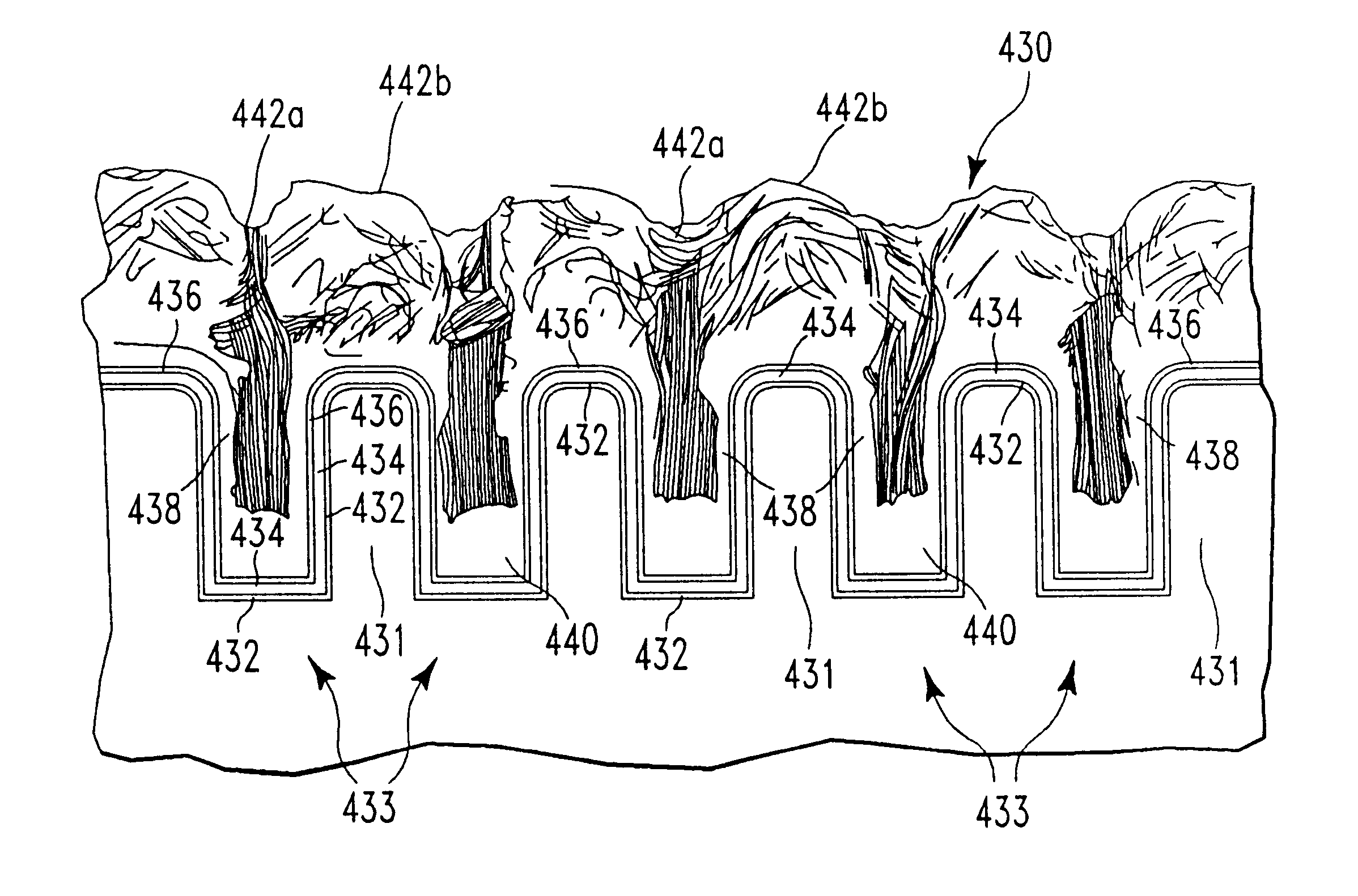
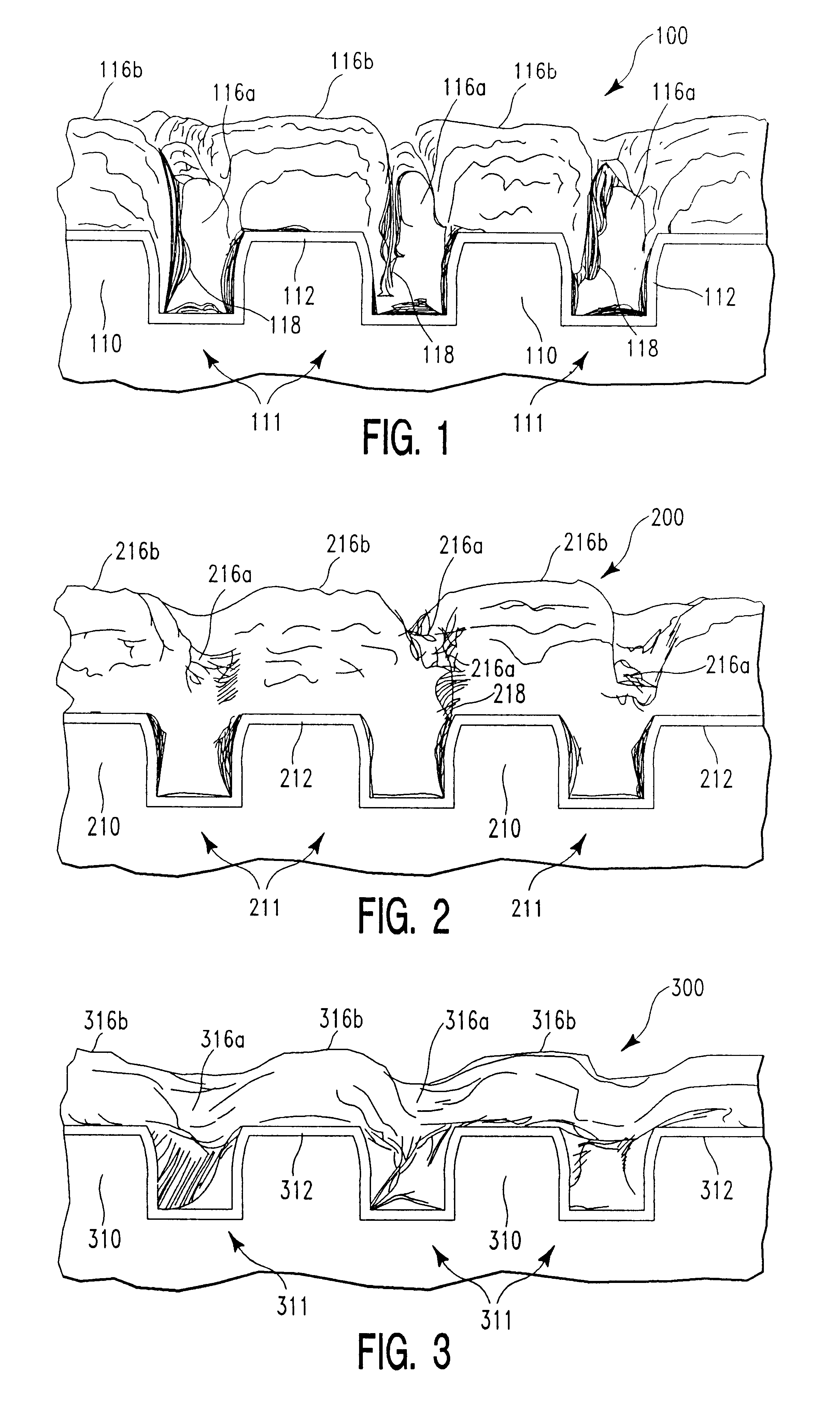
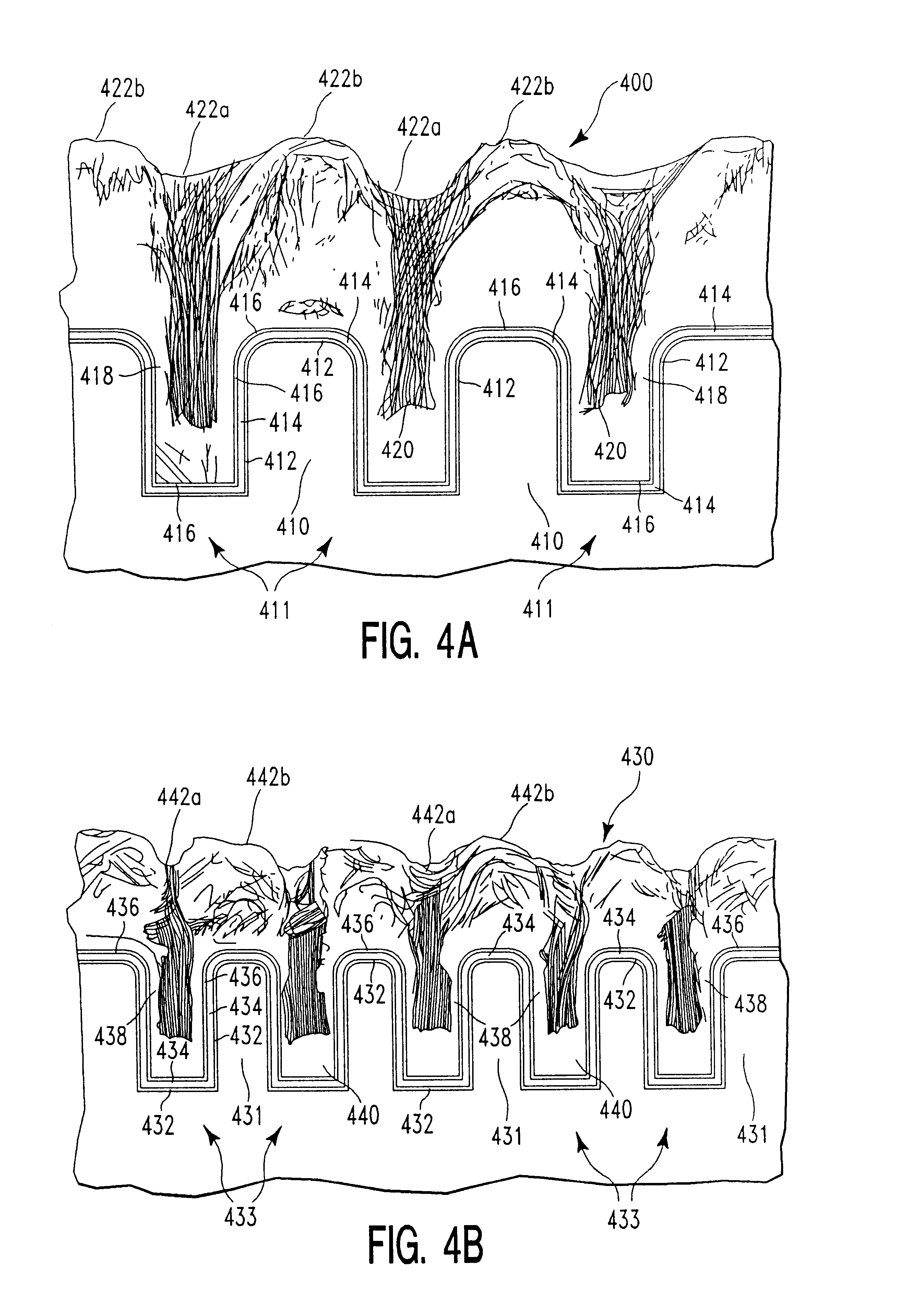
FIGS. 4A and 4B show a schematic of a cross-sectional SEM (400 and 430, respectively) of a silicon oxide substrate (410 and 431, respectively) having copperfilled trenches (411, and 433, respectively) in its surface. A barrier layer (412 and 432, respectively) of Gamma-sputtered tantalum was deposited to a substrate surface thickness of about 800 .ANG. (a sidewall thickness ranging from about 200 .ANG. to about 400 .ANG.) over the silicon oxide substrate. (Had a tantalum nitride barrier layer been used, the preferred method of application would have been reactive IMP sputtering in the presence of nitrogen). A wetting layer (414 and 434, respectively) of Gamma-sputtered aluminum, was deposited to a substrate surface thickness of about 1,000.ANG. (a sidewall thickness ranging from about 100 .ANG. to about 300 .ANG.) over the tantalum barrier layer. This was followed by a second wetting layer of IMP-sputtered copper (416 and 436, respectively), which was applied to a substrate surface ...


PUM

PropertyMeasurementUnit
temperatureaaaaaaaaaa

Abstract

The present disclosure pertains to a method of filling features (typically trenches or vias) on a semiconductor workpiece surface with copper using sputtering techniques previously believed incapable of achieving a copper fill. In particular, when the feature is to be filled with a single, continuous application of sputtered copper, the surface of the substrate to which the sputtered copper is applied should range between about 200° C. and about 600° C.; preferably the surface temperature of the substrate ranges between about 300° C. and about 500° C. When the feature is to be filled using a thin wetting layer of copper, followed by a fill layer of copper, the wetting layer may be applied by sputtering techniques or by other methods such as evaporation or CVD, while the fill layer of copper is applied using sputtering techniques. The thin wetting layer of copper is applied at a substrate surface temperature ranging between about 20° C. to about 250° C., and subsequently the temperature of the substrate is increased, with the application of the sputtered copper fill layer beginning at above at least about 200° C. and continuing while the substrate temperature is increased to a temperature as high as about 600° C. Preferably the substrate temperature during application of the sputtered fill layer ranges between about 300° C. and about 500° C.

Description

1. Field of the InventionThe present invention pertains to the use of sputtering as a means for filling trenches and vias with copper (and alloys thereof). Sputtering techniques include Gamma copper ("long throw" deposition), IMP copper (ionized metal plasma deposition), coherent copper, and traditional (standard) copper deposition. In particular, when the sputtering of copper is carried out under particular process conditions, it is possible to fill feature sizes of 0.4 micron or less having aspect ratios of 1 or greater.2. Brief Description of the Background ArtAs the feature size of semiconductor patterned metal features has become increasingly finer, it is particularly difficult to use the techniques known in the art to provide multilevel metallurgy processing. In addition, future technological requirements include a switch from the currently preferred metallurgy of aluminum to copper, because of copper's lower resistivity and higher electromigration resistance. The standard rea...

Claims


Application Information

Patent Timeline
Patent Type & Authority Patents(United States)
IPC IPC(8): H01L21/70H01L21/768H01L21/285H01L21/02
CPCH01L21/76877H01L21/2855
Inventor DING, PEIJUNCHIANG, TONYCHIN, BARRY L.
Owner APPLIED MATERIALS INC
Why Eureka
Try Eureka