
Monolithic multi-wavelength semiconductor laser unit

a semiconductor laser and monolithic technology, applied in the direction of semiconductor laser arrangement, laser details, laser arrangement, etc., can solve the problems of difficult to make the optical pickup small and light, require a very long time for assembling the optical system, and the injection efficiency of electrons to be very low

Inactive Publication Date: 2003-09-09
KK TOSHIBA
View PDF11 Cites 55 Cited by
  • Summary
  • Abstract
  • Description
  • Claims
  • Application Information

AI Technical Summary

Problems solved by technology

Thus, its configuration becomes complex which results in a problem that it is difficult to make the optical pickup smaller and lighter.
Also, the finely positional adjustments for respective light sources must be done to thereby require a very long time for assembling the optical system.
However, this also brings about a problem. FIG. 2B describes this problem.
The band gap discontinuity and the nonuniform injection cause the injection efficiency of the electron to be very low.
If the laser is operating under such a high voltage, the power dissipation of a circuit for driving the laser is increased, which causes the rated specification, or the standard of the respective circuit elements to be strict, and accordingly makes the manufacturing cost higher, and further generates the heat-flow problem associated with the heat generation resulting from the increase of the power dissipation.
This results in a severe problem on the circuit design.
This results in a reduction of a voltage at which a laser oscillation is excited, and also leads to the low power dissipation of a circuit for driving the first laser.

Method used


Image

  • Monolithic multi-wavelength semiconductor laser unit
  • Monolithic multi-wavelength semiconductor laser unit
  • Monolithic multi-wavelength semiconductor laser unit

Examples


first embodiment

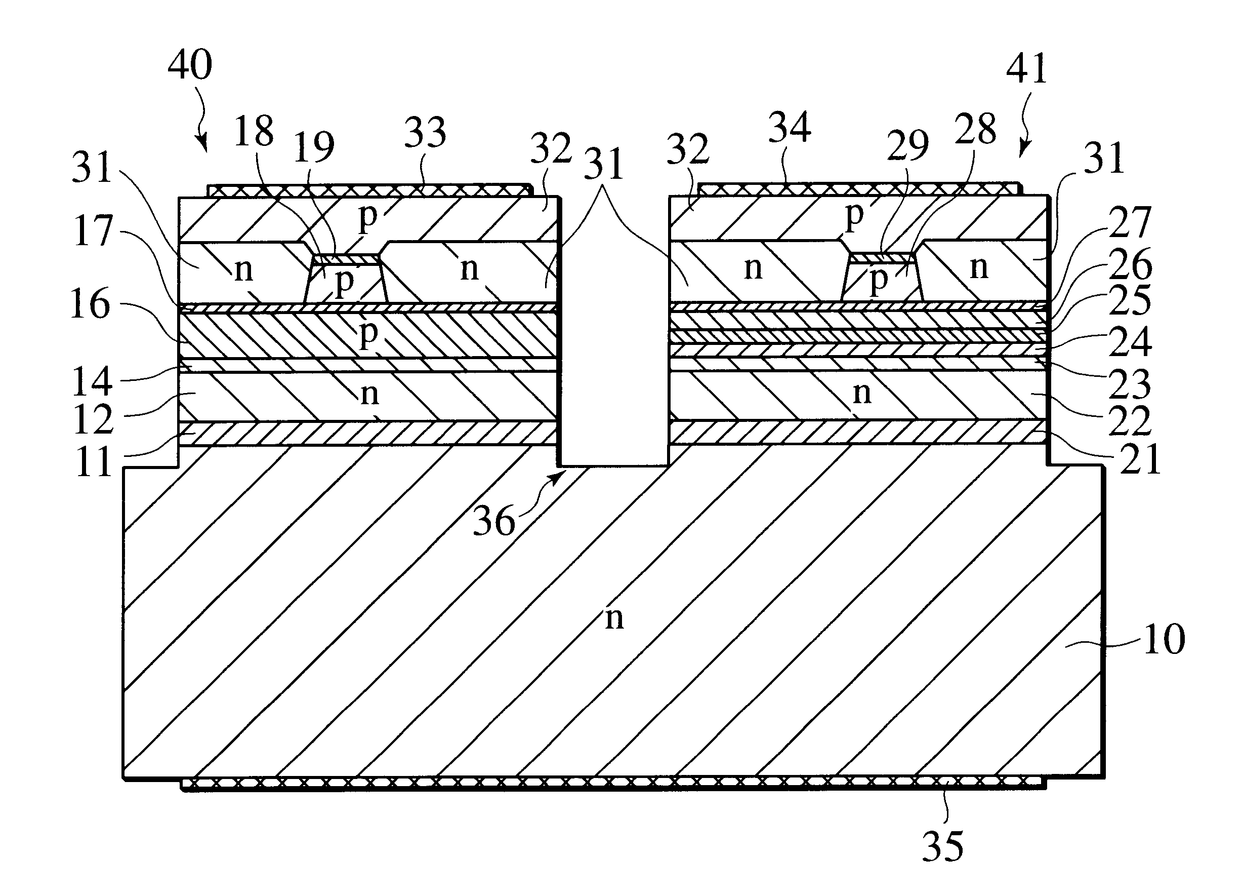
FIG. 3A is a sectional view of a double wavelength semiconductor laser unit emitting radiations with wavelengths of 780 nm and 650 nm according to a first embodiment of the present invention. FIG. 3 shows the sectional view vertical to a ridge stripe direction formed in the double wavelength semiconductor laser unit. As shown in FIG. 3A, a first laser 40 emitting the radiation with the wavelength of 780 nm and a second laser 41 emitting that of 650 nm are merged on the same n-type GaAs crystal substrate 10. In the first laser 40, a second p-type cladding layer (first laser cladding layer of second conductivity type) 18 is delineated to have convex stripe referred to as "ridge", and both sides of the ridge 18 are sandwiched by GaAs current-blocking layers (first laser current-blocking layers) 31. Similarly, in the second lasers 41, second p-type cladding layer (second laser cladding layer of second conductivity type) 28 is delineated to have convex stripe, or the ridge, and both the ...

second embodiment

FIG. 4A is a sectional view of a double wavelength semiconductor laser unit, having oscillation wavelengths of 780 nm and 650 nm, according to a second embodiment of the present invention. FIG. 4A shows the sectional view vertical to a ridge stripe direction of the double wavelength semiconductor laser unit. A first laser 50 emitting the radiation with the wavelength of 780 nm and a second laser 51 emitting that of 650 nm are merged on a same n-type GaAs semiconductor substrate 10. In the first and second lasers 50, 51, second p-type cladding layers 59, 28 are respectively delineated to form convex stripes, or the ridges, and both the sides of the ridges 59, 28 are sandwiched by GaAs current-blocking layers 31, respectively. This structure channels the current into narrowly limited areas of the active layers 55, 24 then generate the striped gain distributions within the active layers 55, 24 Also, the parts of lights penetrated into first p-type cladding layers 57, 26 among lights tr...

third embodiment

FIGS. 5A and 5B show a third embodiment of the present invention, which has a gain waveguide type structure referred to as "a tapered stripe (TAPS) structure". A first laser 200 emitting the radiation with the wavelength of 780 nm and a second laser 201 emitting that of 650 nm are merged on an n-GaAs crystal substrate 224. N-type buffer layers 211, 221 are formed on the crystal substrate 224, correspondingly to the first and second lasers 200, 201. An n-type InGaAlP cladding layer (first laser cladding layer of first conductivity type) 212 is formed on the n-type buffer layers 211. And an n-type InGaAlP cladding layer (second laser cladding layer of first conductivity type) 222 having the compositions equal to the n-type InGaAlP cladding layer 212 is formed on the n-type buffer layer 221. An AlGaAs bulk active layer 214 having thicknesses of 0.01 to 0.1 .mu.m are formed on the n-type InGaAlP cladding layer 212. An MQW active layer 224 sandwiched by waveguide layers 223, 225, is form...


PUM


Abstract

This is a double wavelength semiconductor laser unit having a first laser emitting a light of a first wavelength and a second laser emitting a light of a second wavelength different from the first wavelength. The first and second lasers are merged on a substrate. The first laser has a bulk active layer whose film thickness is 0.01 mum or more and 0.1 mum or less. And the second laser has an MQW active layer constituted by stacked structure composed of a quantum well layer and a barrier layer. By employing the bulk active layer for the first laser, it is possible to reduce the band gap discontinuity induced at a boundary between a cladding layer and the bulk active layer, and then decreases an operational voltage, and further improve the reliability of the first laser.

Description

1. Field of the InventionThe present invention pertains to optical communication, optical interconnects, and optical signal processing employing semiconductor lasers. More particularly, the present invention relates to a monolithic multi-wavelength semiconductor laser unit for outputting laser lights having different wavelengths from a single monolithically integrated semiconductor chip, which can be used in optical memory disk applications.2. Description of the Related ArtAn optical memory disk system is widely put to practical use since it is small-sized and it can record a large capacity of information. Especially, in a digital versatile disk (DVD) system, its practical use has been rapidly promoted as a main system such as a movie, a multi-media application for a next generation and the like. On the other hand, a compact disk (CD) system or a compact disk-recordable (CD-R) system has been conventionally widespread as an optical memory disk. It is desirable that the DVD system ha...

Claims


Application Information

Patent Timeline
IPC IPC(8): H01S5/40H01S5/00H01S5/20H01S5/323
CPCH01S5/4031H01S5/4087H01S5/20
Inventor GEN-EI, KOICHISHIOZAWA, HIDEOTANAKA, AKIRA
Owner KK TOSHIBA
Features
  • Generate Ideas
  • Intellectual Property
  • Life Sciences
  • Materials
  • Tech Scout
  • Unparalleled Data Quality
  • Higher Quality Content
  • 60% Fewer Hallucinations
Learn More