Semiconductor device having junction depths for reducing short channel effect

a short-channel effect and junction depth technology, applied in semiconductor devices, radiation-controlled devices, electrical equipment, etc., can solve the problems of short-channel effect, titanium silicide film forming step, and transistor is ap

Inactive Publication Date: 2004-04-13
SHARP KK
View PDF23 Cites 24 Cited by
  • Summary
  • Abstract
  • Description
  • Claims
  • Application Information

AI Technical Summary

Problems solved by technology

As a result, the transistor is apt to cause short-channel effects involving lowering of threshold voltage, punch-through, and degradation in sub-threshold characteristics.
In PMOS semiconductor devices, there is a general tendency of adopting a surface-channel transistor provided with p-type doping, because the conventional buried-channel transistor with an n-doped gate electrode cannot cope with steping of fine linewidth.
However, the conventional titanium silicide film forming step as above involves problems as given below.
However, there arises worsening of heat resist layerance and causing aggregation of TiSi.sub.2 as compared with a broader linewidth of titanium silicide films.
There is therefore a problem that aggregation is certain to occur in a finer linewidth of titanium silicide films.
This increases junction current leakage through the source and drain regions and lowers the reliability of the gate oxide film.
(6) Where conditions of a heat treatment (anneal) for activation of impurity ions are optimized to meet the p-channel side for suppressing the short-channel effect, crystal-defect restoration on the n-channel side is unsatisfactory, increasing junction current leakage in the n-channel side.
Incidentally, an arsenic ion is heavier than an boron ion, effecting heavier damages in implanting.
However, a silicide formed is positioned closer to a silicide/silicon interface, the junction leakage current increases.
As a result, the gate electrode when applied voltages causes depletion therein, leading to a short-channel effect or reduction of drive power.
On the other hand, if the thickness is thicker than 30 nm, there occurs increase in amount of over-etch prior to deposition of titanium, effecting damages to gate, source, and drain regions.
In such cases, higher energy is required for implantation of ions, resulting in increased implantation damages.
Further, it becomes difficult to form shallow junctions due to increase of dispersion (.sigma.) in implantation profile.
This is because no native oxide film is allowed to grow at the interface of a silicon semiconductor substrate and a titanium film.
If the temperature is lower than 650.degree. C. or the time period is shorter than 10 seconds, the titanium silicide film will be insufficient in growth.
On the other hand, if the temperature is higher than 700.degree. C. or the time period is longer than 60 seconds, there arises tendency of short-circuiting between the gate, the source, and the drain due to growth of the silicide film sideways.
Further, the silicide film is undesirable apt to react with an isolation oxide layer or a spacer oxide film.
If the temperature is lower than 900.degree. C. or the time period is shorter than 10 seconds, the stable C54-crystal will be insufficient in formation.
On the other hand, if the time period is longer than 30 seconds, there arises undesirable tendency of occurring aggregation.
It is noted that if the implant energy is too high there occurs undesirable spreading of the implanted ions sideways to make impo...

Method used


Image

  • Semiconductor device having junction depths for reducing short channel effect
  • Semiconductor device having junction depths for reducing short channel effect
  • Semiconductor device having junction depths for reducing short channel effect

Examples


example 1

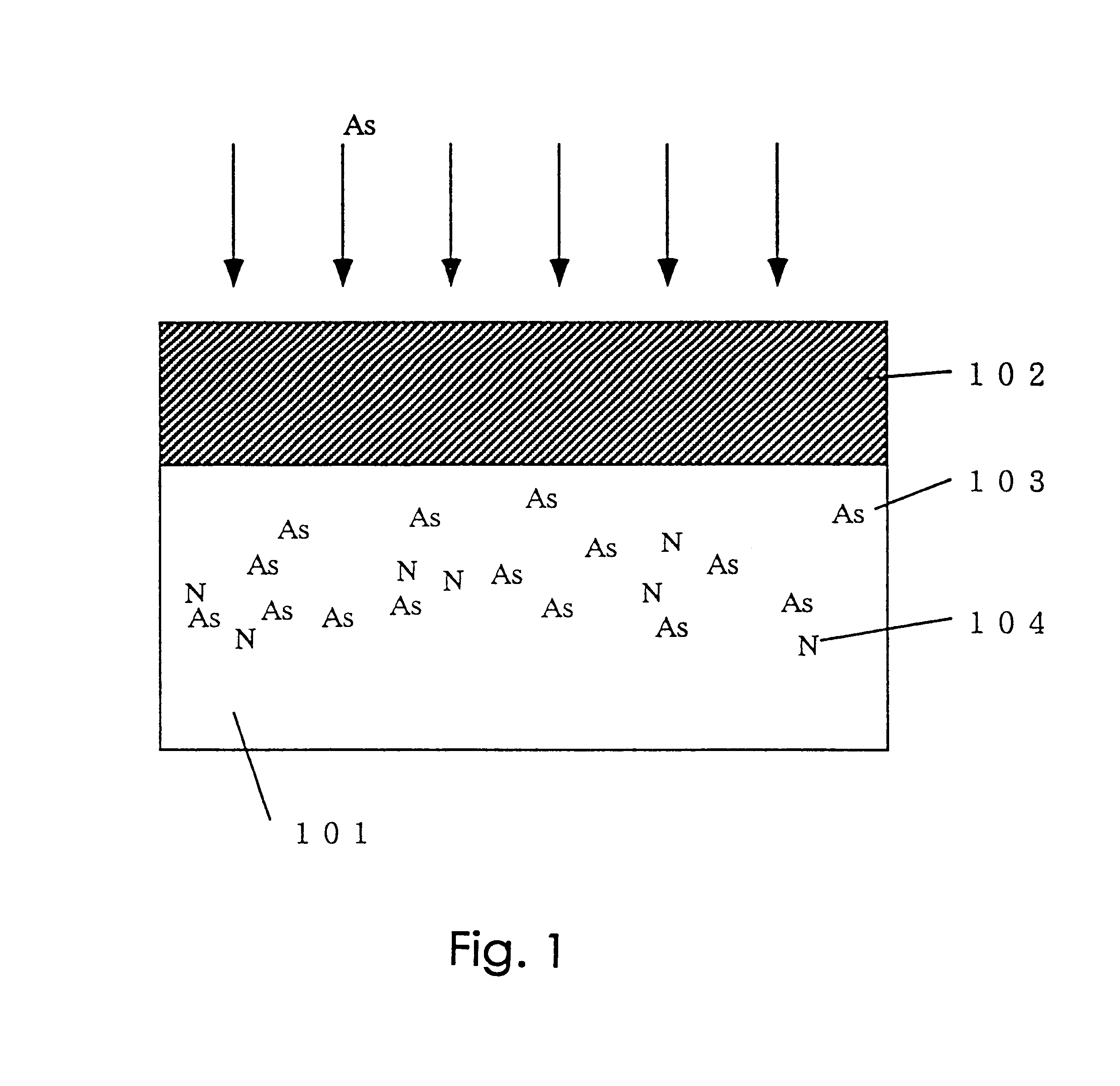
There is illustrated in FIG. 1 a sectional view of a structure according to Example 1 of the present invention.

In Example 1, the surface of a silicon semiconductor substrate 101, before ion implantation, has an oxygen concentration of 1.times.10.sup.18 / cm.sup.3 or less in at least an area where impurity ions are to be implanted.

To realize n oxygen concentration of 1.times.10.sup.18 / cm.sup.3 or less in Example 1, a DZ which is a layer of oxygen-free and defect-free was formed by an IG treatment. The surface of the silicon semiconductor substrate has a structure having a silicon nitride film 102 deposited thereon without a native oxide film (a silicon oxide film) formed therebetween. There existed solely arsenic impurity ions 103 implanted without introducing oxygen atoms and nitride atoms 104 knocked on by the arsenic impurity ions 103 in regions with an oxygen concentration of less than 1.times.10.sup.18 / cm.sup.3 of the silicon semiconductor substrate 101, after implantation of t...

example 2

In Example 2, explanation is made on a method for bringing the oxygen concentration to 1.times.10.sup.18 / cm.sup.3 or below in a polysilicon film such as for a gate electrode, though in Example 1 the DZ was formed oxygen-free and defect-free by the IG treatment.

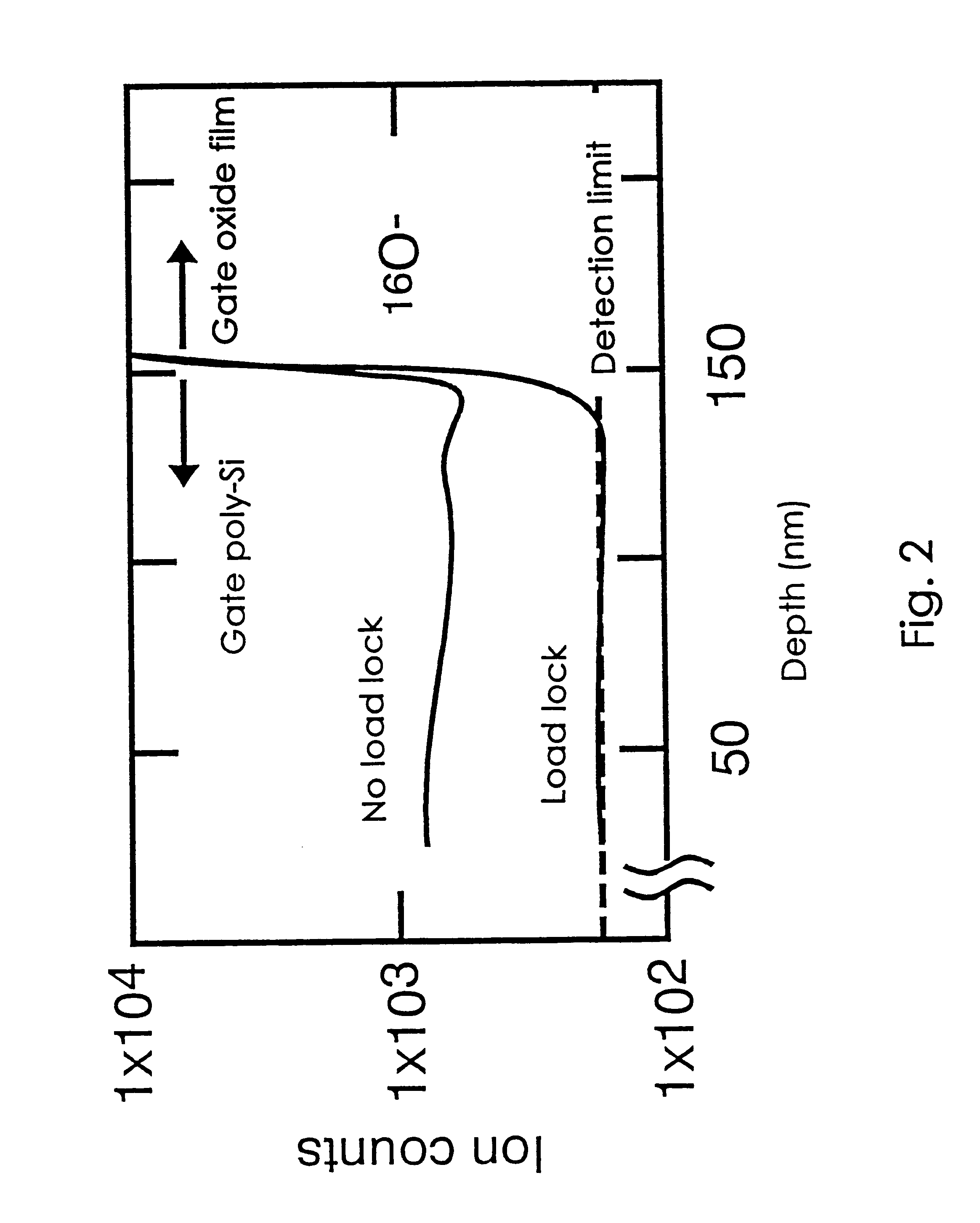
To realize a polysilicon film with an oxygen concentration of 1.times.10.sup.18 / cm.sup.3 or less, a film was formed by using an LP-CVD apparatus having a preparatory evacuation chamber, a load lock chamber, and a deposition furnace connected with carrier system nitrogen-purged. The method of using the LP-CVD (liquid-phase chemical vapor deposition) apparatus is described below.

A semiconductor wafer immediately after being formed with a gate oxide film was accommodated in the preparatory evacuation chamber, and then the preparatory evacuation chamber was evacuated to a pressure of approximately 10.sup.-1 Pa. Thereafter, nitrogen was introduced into the preparatory evacuation chamber, and the semiconductor wafer was transporte...

example 3

FIGS. 3(a)-3(d) and FIGS. 4(e) and 4(f) are sectional views showing steps for fabricating the semiconductor device according to the invention.

First, silicon semiconductor substrate 30 of a p-type was subjected to an IG treatment form a DZ 302 which has a surface free of oxygen and defects, as shown in FIG. 3(a). Then, a silicon nitride film 303 was formed to a thickness of approximately 5-30 nm over the surface of the silicon semiconductor substrate by the use of an LP-CVD apparatus. The LP-CVD apparatus is provided with a cassette chamber, a load-lock chamber, and a deposition furnace, as shown in FIG. 3(b). Arsenic ions as an impurity were implanted through the silicon nitride film 303 into the silicon semiconductor substrate, as shown in FIG. 3(c), under conditions of a dose of approximately 5.times.10.sup.14 -5.times.10.sup.15 / cm.sup.2 with an implant energy of 40 keV-60 keV. On this occasion, nitride atoms 305 besides arsenic ions 304 were introduced through knocking-on into t...


PUM


Abstract

A semiconductor device and a fabrication method thereof are disclosed. A silicon nitride film is formed over a silicon semiconductor substrate. Impurity ions are then implanted into desired areas of the silicon semiconductor substrate, so that nitrogen atoms and silicon atoms from the silicon nitride film are incorporated into the surface of the silicon semiconductor substrate together with introduction of impurity ions. The silicon semiconductor substrate has a minimized content of oxygen mixed thereinto and restored crystal defects filled by nitrogen atoms upon implanting of impurity ions. The fabricated semiconductor device is free from a trade-off relation between gate-electrode depletion and junction current leakage, and short-channel effects.

Description

1. Field of the InventionThis invention relates to a semiconductor device and a fabrication method thereof, and more particularly to a method for forming a titanium silicide film which is low in electric resist layerance and excellent in heat resist layerance, and a semiconductor device, such as a salicide CMOS transistor, which is reduced in junction leakage currents and suppressed in short-channel effect for raising drive power, and a method of fabricating the same.2. Related ArtIn insulated-gate field effect transistors employed in semiconductor integrated circuits currently available, there is reduction of depletion-layer electric charges carried by a gate electrode relative to the total amount of depletion-layer electric charges, as the device miniaturizes. As a result, the transistor is apt to cause short-channel effects involving lowering of threshold voltage, punch-through, and degradation in sub-threshold characteristics. One factor of such phenomenon is attributable to dee...

Claims


Application Information

Patent Timeline
IPC IPC(8): H01L21/265H01L21/285H01L21/336H01L21/02H01L21/70H01L21/28H01L21/8238
CPCH01L21/26506H01L21/2652H01L21/26526H01L21/28052H01L21/28518H01L21/823807H01L29/665H01L29/6659H01L21/2658
Inventor IWATA, HIROSHINAKANO, MASAYUKIHAYASHIDA, SHIGEKIKAKIMOTO, SEIZOUMATSUOKA, TOSHIMASA
Owner SHARP KK
Why Eureka
Try Eureka