Imaging device and digital camera using the imaging device

a technology of imaging device and lens barrel, which is applied in the direction of printers, instruments, cameras, etc., can solve the problems of insufficient security of peripheral light, inability to secure the optical performance of image sensors, and difficulty in setting the pupil of the microlens, so as to reduce the cost of imaging devices, improve the degree of freedom of lens barrel structure, and thin optical system

Inactive Publication Date: 2004-04-27
MINOLTA CO LTD
View PDF14 Cites 28 Cited by
  • Summary
  • Abstract
  • Description
  • Claims
  • Application Information

AI Technical Summary

Benefits of technology

Another object of the present invention is to provide an imaging device that is compact and can be manufactured at low cost although having a high-performance and high-magnification zoom lens system.
Further, it is desirable that the first lens unit Gr1 be fixed with respect to the image plane during zooming. Since the first lens unit Gr1 includes the reflecting surface, moving it requires a large space, and in particular, when the reflecting surface comprises a prism, it is necessary to move a prism having a large weight, so that a heavy burden is placed on the driving mechanism. Moreover, by the first lens unit Gr1 being fixed with respect to the image plane during zooming, an optical system whose overall length does not vary can be obtained. Moreover, since the lens barrel structure can be simplified, cost reduction of the imaging device can be attained. Further, by adopting the structure that the first lens unit Gr1 is fixed during zooming, particularly in digital cameras, it is easy to initialize the control system for controlling the lens units movable during zooming, so that the time necessary for the camera to become ready to photograph when the main power is turned on can be reduced.

Problems solved by technology

However, in these zoom lens systems, since the exit pupil of the lens system in the shortest focal length condition is situated comparatively near the image plane, it does not match with the pupil of the microlens provided so as to correspond to each pixel of the image sensor having high pixels, so that a sufficient quantity of peripheral light cannot be secured.
In addition, since the position of the exit pupil largely varies during zooming, the setting of the pupil of the microlens is difficult.
Further, since required optical performance such as spatial frequency characteristics is completely different between silver halide film and image sensors to begin with, optical performance required of image sensors cannot be sufficiently secured.
It is difficult to reduce the overall size of imaging devices having a zoom lens system unless the zoom lens system taking up the largest space in volume is optimized.
Moreover, although demand for cost reduction of these imaging devices are strong, there is a limitation to the cost reduction.

Method used


Image

  • Imaging device and digital camera using the imaging device
  • Imaging device and digital camera using the imaging device
  • Imaging device and digital camera using the imaging device

Examples


example 2

EXAMPLE 3

example 4

EXAMPLE 5

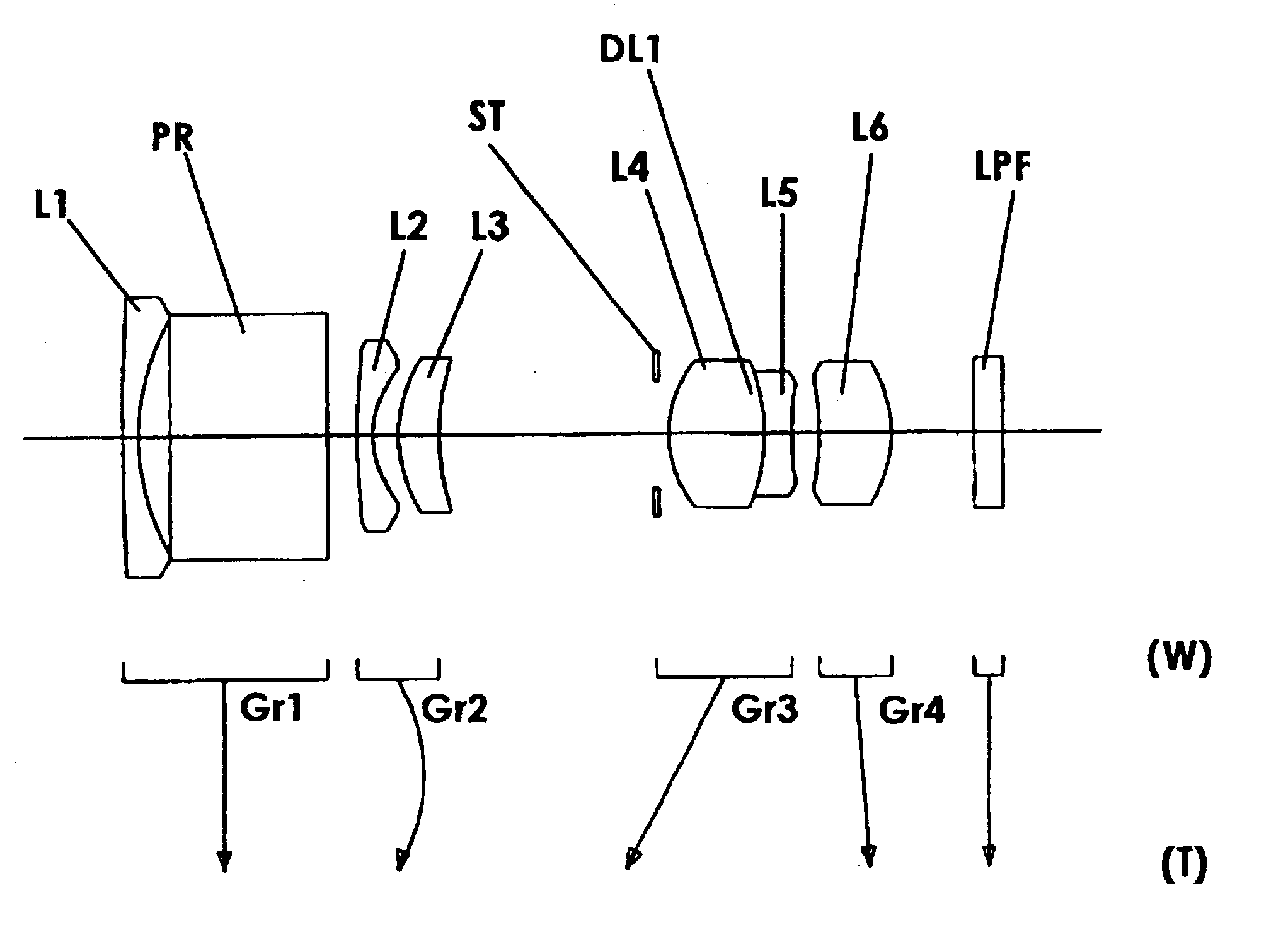
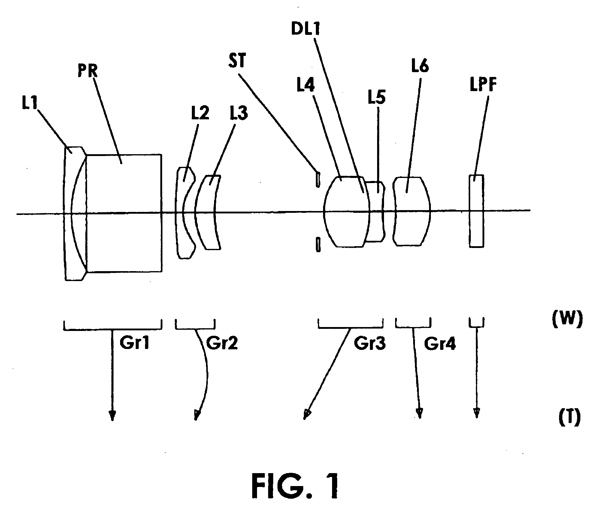
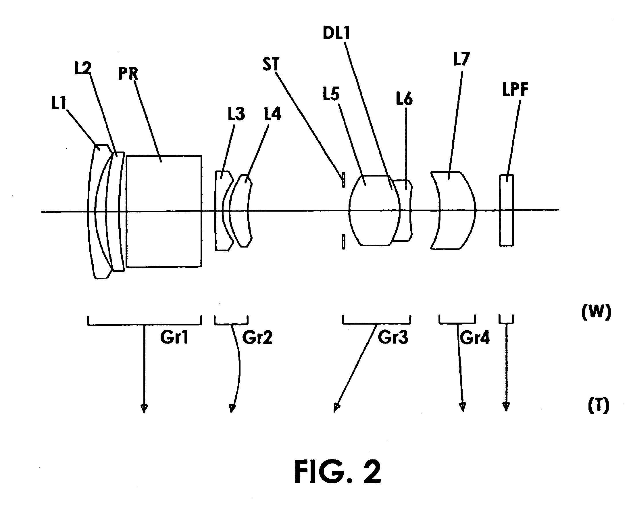
FIGS. 6A to 6I through 10A to 10I which are graphic representations of aberrations of the first to the fifth examples show aberrations of the zoom lens systems of the examples in in-focus state at infinity. In these figures, (W), (M) and (T) show aberrations (from the left, spherical aberration, sine condition, astigmatism and distortion; Y'(mm) is the maximum image height [corresponding to the distance from the optical axis] on the image sensor) in the shortest focal length condition, in the middle focal length condition and in the longest focal length condition, respectively. In the graphic representations of spherical aberration, the solid line (d) shows spherical aberration to the d-line, the chain line (g) shows spherical aberration to the g-line, the chain double-dashed line (c) shows spherical aberration to the c-line, and the broken line (SC) shows sine condition. In the graphic representations of astigmatism, the broken line (DM) shows astigmatism on the meridional...


PUM


Abstract

An imaging device has a zoom lens system having a plurality of lens units and forming an optical image of an object so as to continuously optically zoom by varying distances between the lens unit; and an image sensor converting the optical image formed by the zoom lens system to an electric signal. The zoom lens system has from an object side, a first lens unit being overall negative and including a reflecting surface that bends a luminous flux substantially 90 degrees; and a second lens unit disposed with a variable air distance from the first lens unit, and having an optical power, and wherein at least one lens element made of resin is included in the entire lens system.

Description

This application is based on application No. 2002-196168 filed in Japan on Jul. 4, 2002, the content of which is hereby incorporated by reference.The present invention relates to an imaging device having an image sensor that converts, to electric signals, optical images formed on the light receiving surface of a charge coupled device (CCD), a complementary metal-oxide semiconductor (CMOS) sensor or the like, and more particularly, to an imaging device which is a principal element of cameras incorporated in or externally attached to digital cameras, personal computers, mobile computers, mobile telephones, personal digital assistances (PDAs) and the like. Specifically, the present invention relates to a compact imaging device having a zoom lens system.DESCRIPTION OF THE PRIOR ARTIn recent years, digital cameras have been rapidly becoming widespread that convert an optical image to electronic signals by using an image sensor such as a CCD or a CMOS sensor instead of silver halide film,...

Claims


Application Information

Patent Timeline
Patent Type & Authority Patents(United States)
IPC IPC(8): H04N5/225G03B11/00G02B15/177G02B15/20H04N101/00
CPCG02B15/177H04N5/2254G02B15/142G02B15/1455G02B15/1445
Inventor HAGIMORI, HITOSHIYAMAMOTO, YASUSHIYAGYU, GENTAISHIMARU, KAZUHIKO
Owner MINOLTA CO LTD
Why Eureka
Try Eureka