Liner with poor step coverage to improve contact resistance in W contacts

a technology of w contacts and step coverage, applied in the direction of basic electric elements, electrical apparatus, semiconductor devices, etc., can solve the problem of widening the resistance spread

Inactive Publication Date: 2004-05-11
IBM CORP +1
View PDF13 Cites 24 Cited by
  • Summary
  • Abstract
  • Description
  • Claims
  • Application Information

AI Technical Summary

Benefits of technology

Another object of the present invention is to provide, in the case of a dual damascene, where W interconnects contacting underlying metal layers and wherein the contact resistance is a problem, a liner with poor step coverage to improve the contact resistance in the W contacts.
A further object yet still of the present invention is to provide, in the case of both single and dual damascene W interconnects contacting underlying metal layers and where the contact resistance is a problem because W does not stick to oxide and thereby requires a liner to secure adhesion to the surface and sidewall of the wafer, a replacement of the traditional liner with a liner that decreases the contact resistance and lessens the resistance spread, through the use of a very poor step coverage PVD TiN coating, so that coating of the surface is provided without coverage at the via bottom.

Problems solved by technology

Further, in both single and dual damascene tungsten (W) interconnects contacting unlying metal layers, the contact resistance poses a problem because the W does not stick to oxide, thereby requiring the use of a liner to provide appropriate adhesion on the surface of the wafer; however, the problem is that the liner, which is generally made of TiN or a nitrogen treated Ti increases the contact resistance and also widens the resistance spread.

Method used


Image

  • Liner with poor step coverage to improve contact resistance in W contacts
  • Liner with poor step coverage to improve contact resistance in W contacts

Examples


Embodiment Construction

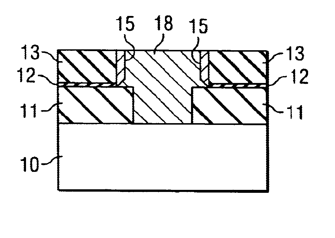
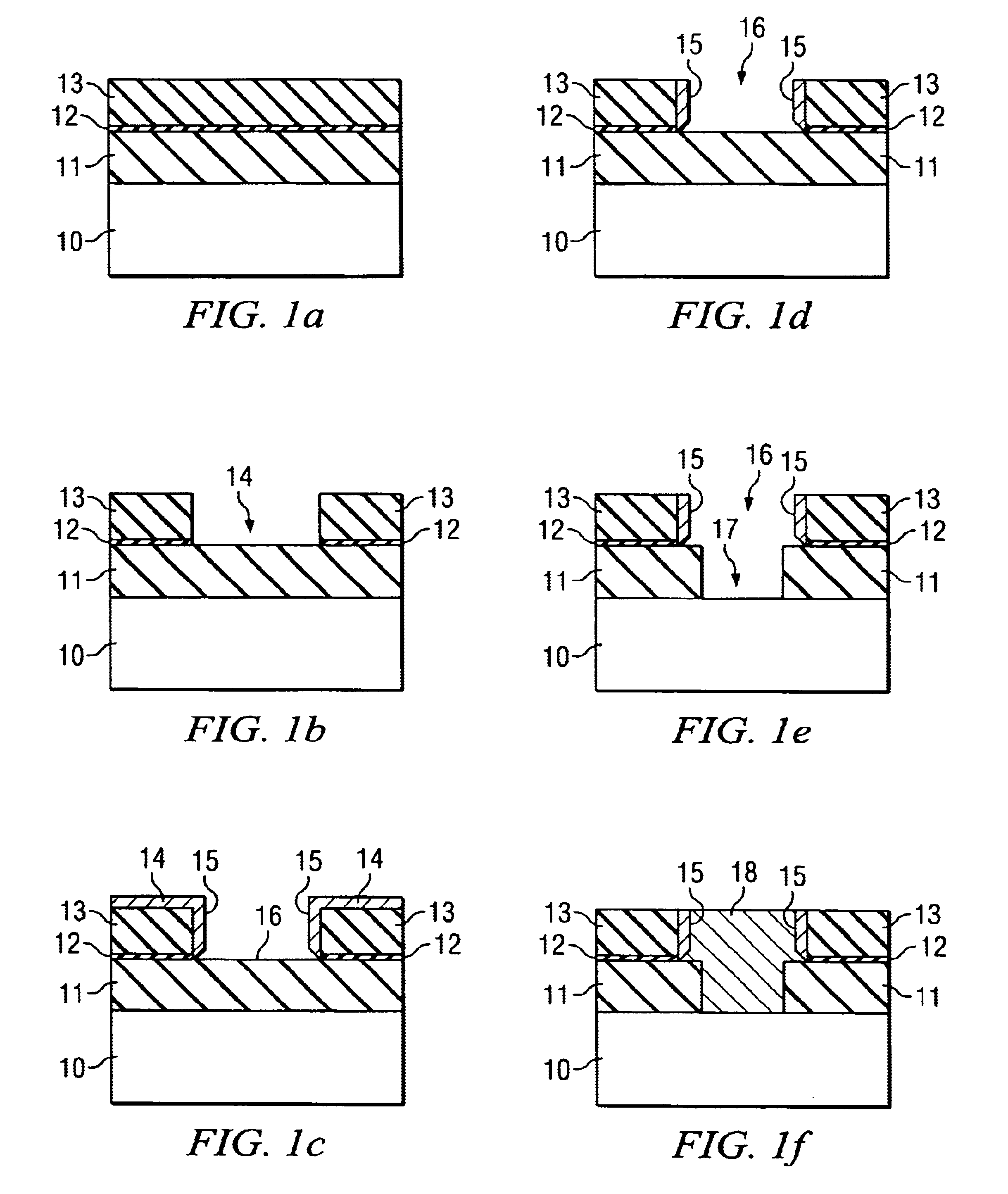
The present invention is directed to fabricating and manufacturing a current carrying metal filled contact / vias of sub-micron diameter using a liner with poor step coverage to improve the contact resistance in W contacts. The process can be used in MOSFET or CMOS or any high density semiconductor device presently being manufactured in the semiconductor industry; however, only those specific areas unique to comprehension of this invention will be described.

In general, a conductive plug filling a via hole is formed by depositing an interlayer dielectric (ILD) on a conductive layer comprising at least one conductive layer comprising at least one conductive pattern, forming an opening through the ILD by photolithographic and etching techniques, and filling the opening with a conductive material. Excess conductive material on the surface of the ILD is generally removed by chemical mechanical polishing (CMP). One such method is known as the single damascene technique and entails the forma...


PUM

PropertyMeasurementUnit
resistanceaaaaaaaaaa
adhesionaaaaaaaaaa
electrically conductiveaaaaaaaaaa

Abstract

A method of filling a damascene structure with liner and W characterized by improved resistance and resistance spread and adequate adhesion comprising: a given damascene structure coated by a liner which purposely provides poor step coverage into the afore mentioned structure, followed by a CVD W deposition, and followed by a metal isolation technique.

Description

1. Field of the InventionThe present invention relates to the use of a liner purposely having poor step coverage to improve the properties in W vias. The liner is characterized by appropriate adhesion for the W layer without increasing or widening the resistance values and spread respectively.2. Description of The Prior ArtIn general, semiconductors and integrated circuit devices will comprise a silicon substrate and a doped region(s) disposed in the semiconductor in which there are source or drain connections, separated by a gate or gate control region. Metal connections are made to the source, gate, and drain electrodes by interconnects that are supported over the substrate by an interlayer dielectric material.Electrical connections are made between different layers by patterning and etching the dielectric to form contact and via openings. The openings are generally filled with electrically conductive materials of plugs made of W (tungsten) that contact previously doped regions, p...

Claims


Application Information

Patent Timeline
Patent Type & Authority Patents(United States)
IPC IPC(8): H01L21/70H01L21/768
CPCH01L21/76807H01L21/76844H01L2924/0002H01L2924/00
Inventor IGGULDEN, ROY C.SHAFER, PADRAICROBL, WERNERWONG, KWONG HON
Owner IBM CORP
Why Eureka
Try Eureka