

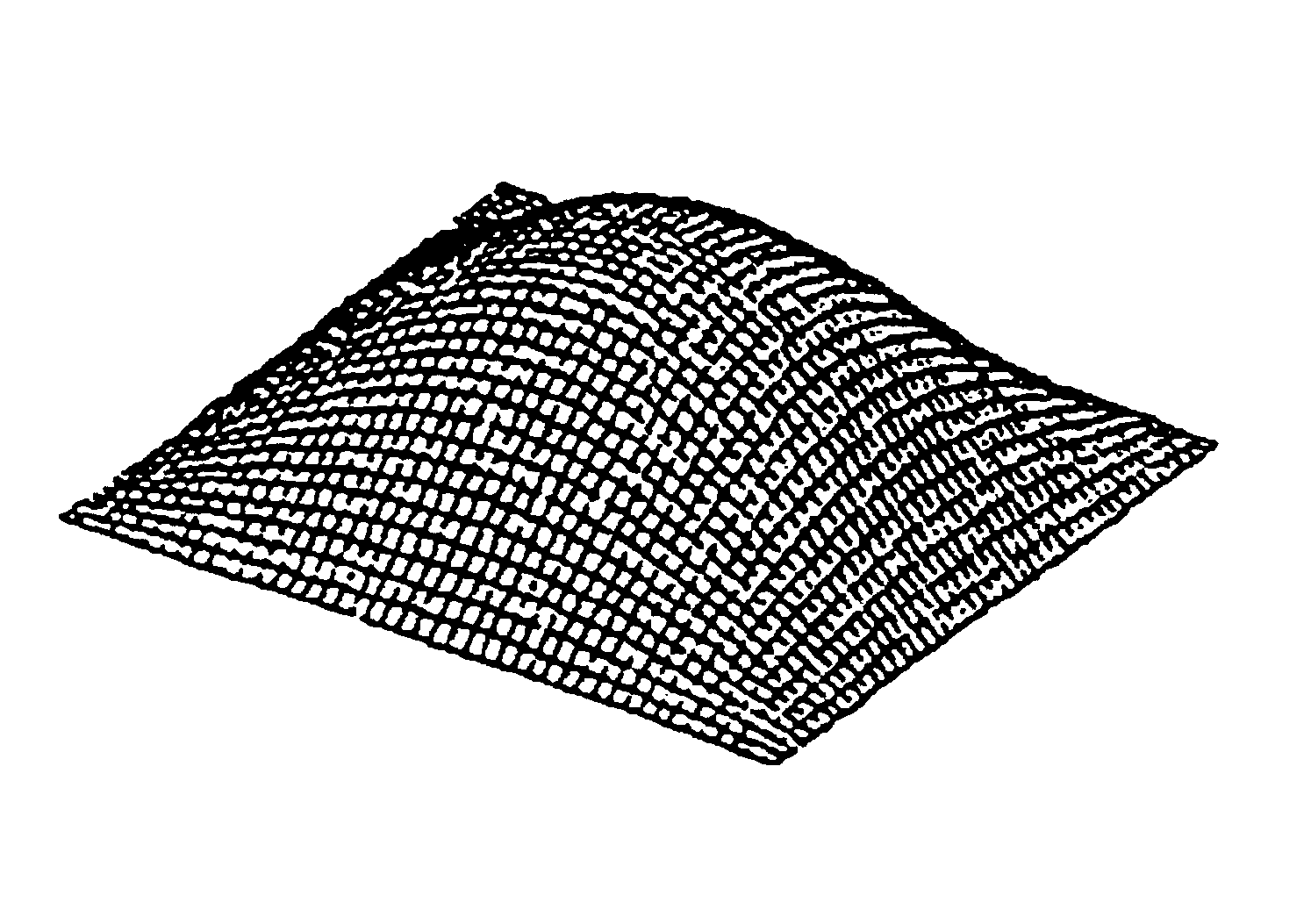
Shape of microdot mark formed by laser beam and microdot marking method
a laser beam and microdot technology, applied in the direction of identification means, instruments, signs, etc., can solve the problems of reducing and reducing so as to prevent the loss of thermal energy, the number of dots to be marked, and reduce the size of the do
- Summary
- Abstract
- Description
- Claims
- Application Information
AI Technical Summary
Benefits of technology
Problems solved by technology
Method used
Image

Examples
Embodiment Construction
Preferred Examples of the invention will be specifically described hereinbelow in conjunction with comparative shapes with reference to the accompanying drawings.
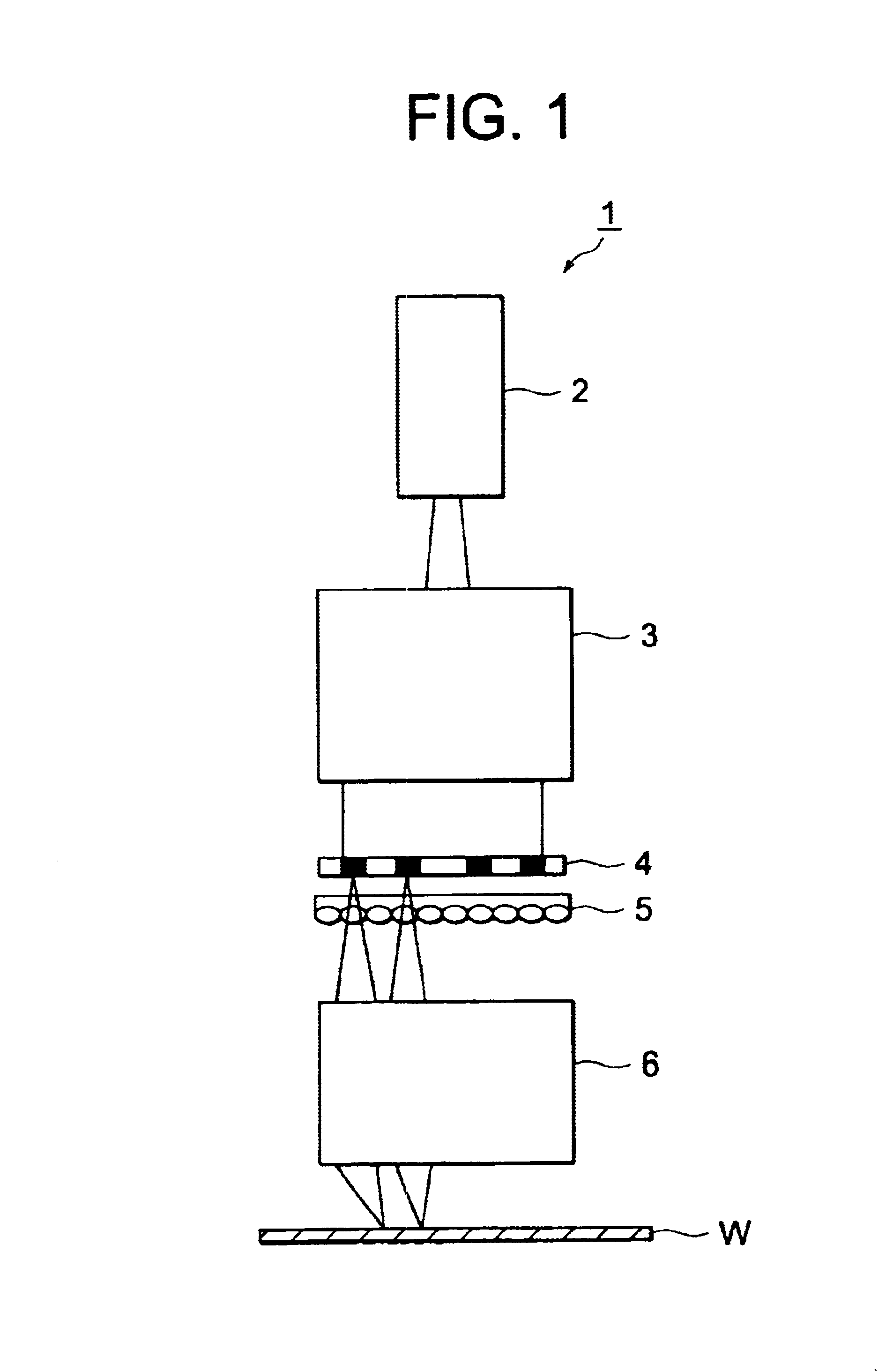
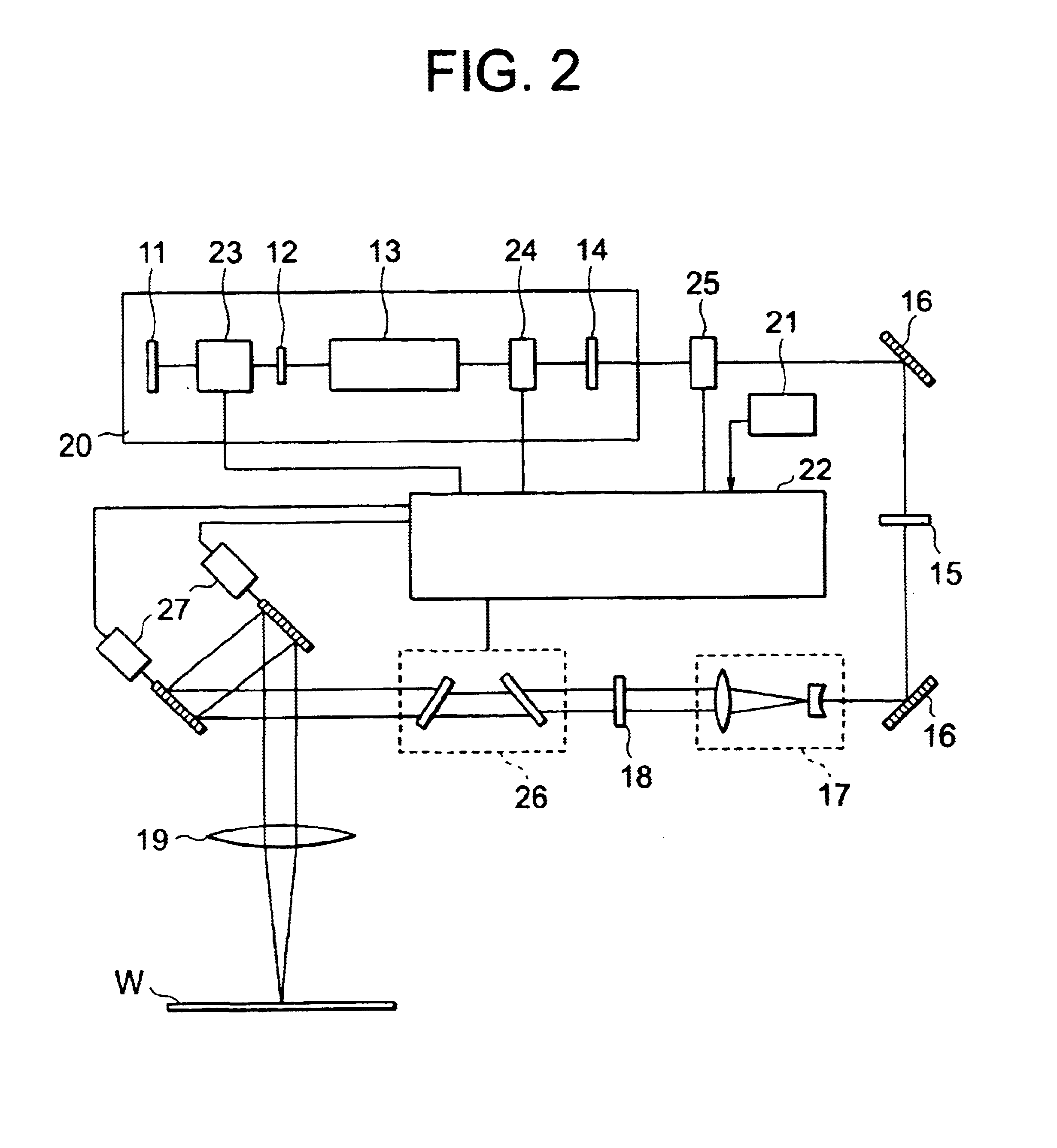
FIG. 1 is a diagram schematically showing an embodiment of a laser marking apparatus for forming a microdot mark of the invention.
In FIG. 1, reference numeral 2 denotes a laser oscillator; 3 a beam homogenizer; 4 a liquid crystal mask, 5 a bean profile converter; and 6 a condenser lens unit, and reference character W indicates an article to be marked. In the embodiment, as the article W to be marked, a semiconductor wafer is used as an example. The semiconductor wafer W in the embodiment includes not only a silicon wafer but also a general wafer such as a wafer on which an oxide film or a nitride film is formed, an epitaxial semiconductor wafer, and further a semiconductor wafer formed by using gallium arsenide or an indium phosphorus compound.
In the laser marking apparatus 1, a laser beam having a Gaussian energy density d...
PUM
| Property | Measurement | Unit |
|---|---|---|
| length | aaaaa | aaaaa |
| length | aaaaa | aaaaa |
| height | aaaaa | aaaaa |
Abstract
Description
Claims
Application Information