
Chip electronic component

a technology of electronic components and chips, applied in the direction of positive temperature coefficient thermistors, ceramic layered products, transportation and packaging, etc., can solve the problems of deterioration of properties, metal coatings on parts of elements, and penetration into ceramic elements

Inactive Publication Date: 2004-09-14
MURATA MFG CO LTD
View PDF2 Cites 9 Cited by
  • Summary
  • Abstract
  • Description
  • Claims
  • Application Information

AI Technical Summary

Benefits of technology

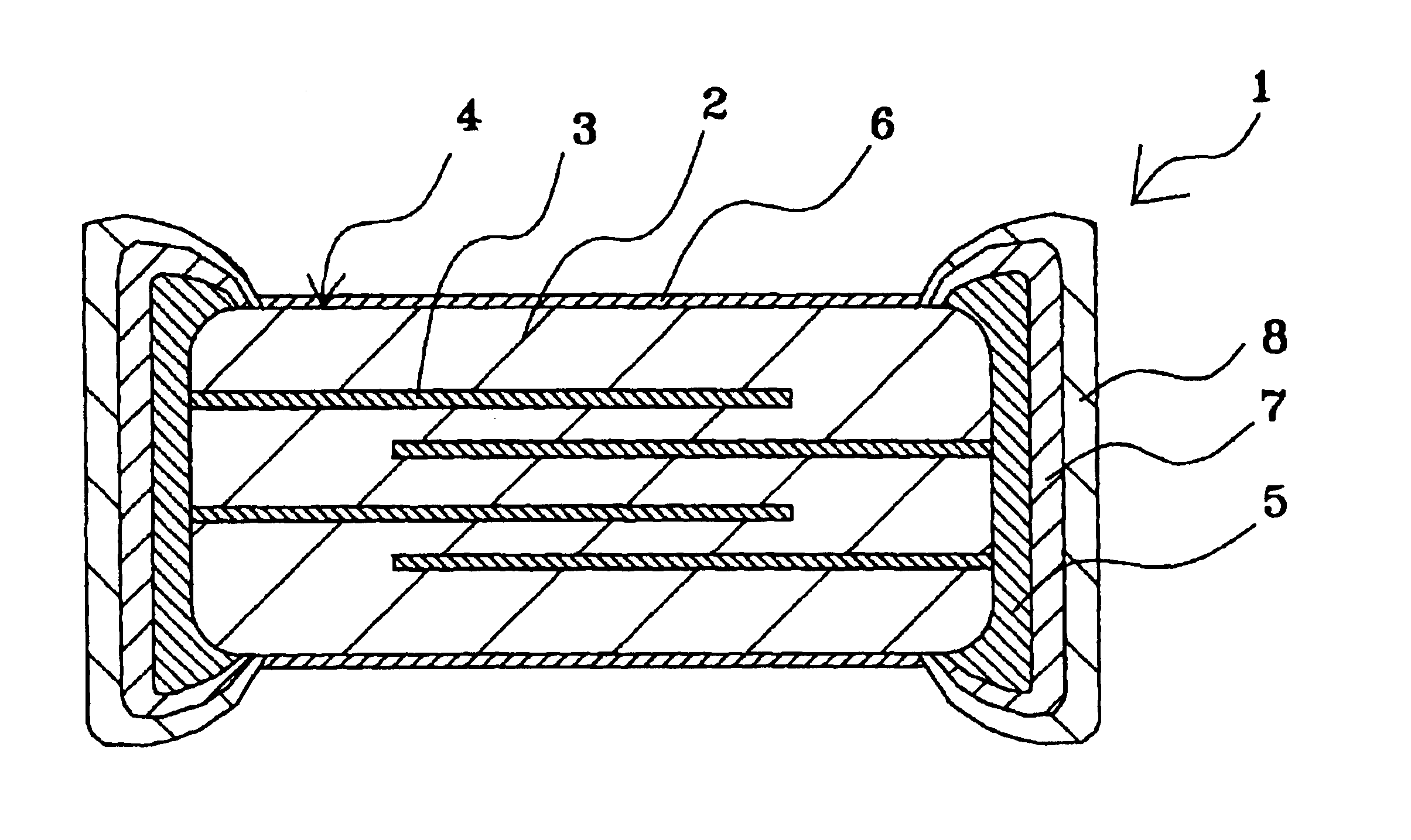
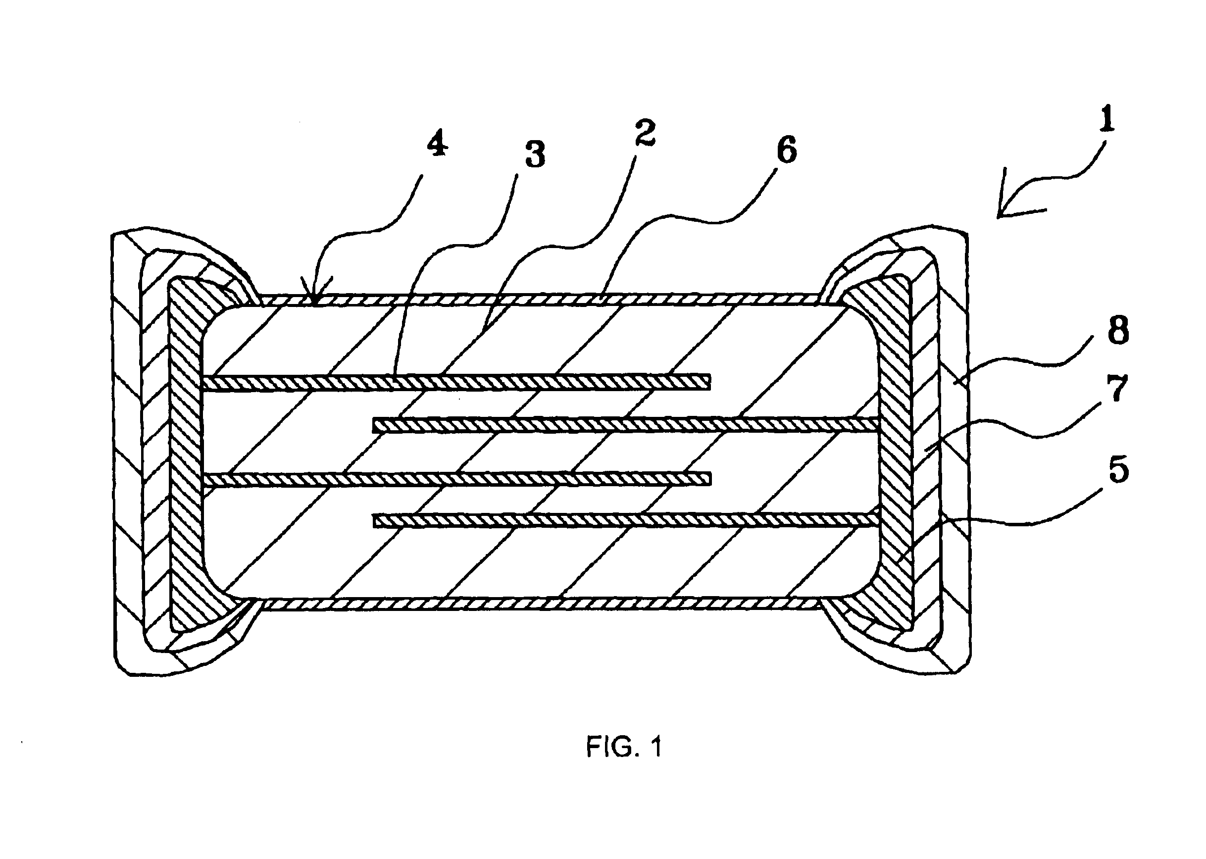
The present invention relates to a chip electronic component that includes a ceramic element and terminal electrodes with metal coatings. To prevent soldering erosion, a glass layer is formed on the ceramic element, but this leads to a problem of reduced dielectric strength due to the formation of cracks in the glass layer. To solve this problem, the invention proposes a chip electronic component with a glass layer that contains at least two species of alkali metal elements. The amount of alkali metal elements in the glass layer is greater than or equal to 20 atomic percent of the atomic total amount of elements, except oxygen. This glass layer prevents metal coatings from being formed on areas of the ceramic element where the terminal electrodes are not disposed, while also preventing cracks in the glass layer. The chip electronic component with this glass layer has a sufficient dielectric strength and prevents plating solution from permeating the ceramic element. The invention also provides a method for preventing deterioration in the dielectric strength of a chip electronic component caused by the formation of cracks in the glass layer.

Problems solved by technology

However, when a ceramic element has a small sintered density, even if it is insulative, a plating solution permeates into the ceramic element and deteriorates its properties.
Furthermore, when terminal electrodes sintered onto a semi-conductive ceramic element are subjected to electroplating, there is a problem that metal coatings are also formed on portions of the element on which the terminal electrodes are not disposed.
However, a chip electronic component having a glass layer thereon containing a large quantity of one of the alkali metal elements has proved to drop extremely in the dielectric strength according to the energization test.
More specifically, when a large amount of alkali metal elements are contained in a glass material to form a glass layer, alkali metal elements are ionized and therefore ionic conduction takes place, whereby an electric current is allowed to flow on the surface of the chip electronic component and the dielectric strength is seriously deteriorated.
When the ratio is outside of the range, the effectiveness, which can be obtained by giving two or more different occupied positions, is weakened.

Method used


Image

  • Chip electronic component
  • Chip electronic component

Examples


Embodiment Construction

BaTiO.sub.3, TiO.sub.2, Sm.sub.2 O.sub.3 and MnCO.sub.3 were prepared as raw materials and then compounded so that the following formula was satisfied:

(Ba.sub.0.997 Sm.sub.0.003)TiO.sub.3 +0.0005 Mn.

After pure water was added, the compounded raw material powder was mixed and pulverized for 16 hours together with zirconia balls, and after drying it was sintered temporarily at 1,200.degree. C. for two hours and pulverized to form a temporarily-sintered powder. To this temporarily-sintered powder, an organic binder, a dispersant and water were added and mixed for ten hours together with zirconia balls to form a ceramic slurry. This ceramic slurry was formed into sheets by a doctor blade process and dried to form ceramic green sheets. Next, Ni electrode paste was applied onto a principal face of each ceramic green sheet by a screen printing process so as to form a desired pattern. The ceramic green sheets were stacked so that the Ni electrode paste patterns were placed opposite to each ...


PUM

PropertyMeasurementUnit
ionic radiusaaaaaaaaaa

Abstract

A chip electronic component including a ceramic element and terminal electrodes with metal coating thereon formed on the surface of the ceramic element. A glass layer is formed on a part of the surface of the ceramic element where the terminal electrodes are not formed. A glass material for the glass layer contains at least two species of alkali metal elements selected from Li, Na and K, and the total amount of the alkali metal elements is greater than or equal to 20 atomic percent of the total amount of elements except oxygen contained in the glass material.

Description

1. Field of the InventionThe present invention relates to a chip electronic component including a ceramic element and terminal electrodes having a metal coating disposed on the ceramic element.2. Description of the Related ArtIn recent years, needs for surface mountable electronic components have been increasing and therefore needs for chip electronic components have also been increasing. For example, a monolithic PTC thermistor is manufactured according to the following procedure: ceramic green sheets containing BaTiO.sub.3 and conductive paste containing conductive powder such as Ni are alternately laminated, and sintered integrally to form a ceramic element. Then, terminal electrodes containing Ag or the like are each formed on the end faces of the ceramic element by a printing process.A chip electronic component, manufactured according to the above procedure, is normally soldered when it is mounted on a substrate. During the soldering step, terminal electrodes of the component a...

Claims


Application Information

Patent Timeline
Patent Type & Authority Patents(United States)
IPC IPC(8): H01C7/18H01C7/02
CPCC04B35/4682H01C7/18H01C7/021C04B2235/3224C04B2235/3262Y10T428/24926Y10T428/24917H01C7/02
Inventor KISHIMOTO, ATSUSHINIIMI, HIDEAKIANDO, AKIRA
Owner MURATA MFG CO LTD
Learn More