Method for forming polyatomic layers

a polyatomic layer and layer technology, applied in the direction of basic electric elements, semiconductor/solid-state device manufacturing, electric apparatus, etc., can solve the problems of low efficiency, difficult to apply a method of increasing the charge storage area of capacitors, and increase production costs, so as to reduce the number of process steps and increase the deposition speed

Inactive Publication Date: 2004-10-05
SK HYNIX INC
View PDF3 Cites 97 Cited by
  • Summary
  • Abstract
  • Description
  • Claims
  • Application Information

AI Technical Summary

Benefits of technology

Therefore, a method for forming a polyatomic layer, capable of reducing a number of process steps and increasing deposition speed is disclosed.
In this mixed deposition method, various elements having respective characteristics, such as thermal decomposition, deposition speed, incorporation efficiency and sticking coefficient, are deposited independently with the ALD method and the CVD method. Therefore, it is possible to obtain characteristics, such as good step coverage and abilities of containing impurities and controlling composition, provided by the ALD. In addition, it is possible to improve the deposition speed and to shorten the process time by the CVD.

Problems solved by technology

However, in case the structure of a capacitor is made complicated just to increase its charge storage area, there are problems that the production cost goes up and that the efficiency declines due to the complex manufacturing process.
Therefore, it is hard to apply a method of increasing the charge storage area of a capacitor by forming it in three-dimensional and fulfilling capacitance to a DRAM device over a 1 Gb class.
But, this Ta.sub.2 O.sub.5 dielectric layer creates a problem as the amount of leakage current increases.
However, in case of forming the multitudinous thin film composed of various atoms with the sputtering method, it is not easy to obtain the uniformity of the thin film, because the various atoms need the different optimum condition for depositing.
Therefore, the sputtering method has limitations to be applied to form fine patterns.
However, it is difficult to control thermal stability of the atoms because of the rapid gas reaction and the physical and chemical properties of the thin film are deteriorated.
If the atomic ratios of the BST layer or the STO layer are quite different from each stoichiometry, the BST layer or the STO layer cannot have the perovskite structure even after an annealing process, and it is impossible to increase the dielectric constant of each layer.
However, it is difficult to obtain a common process condition in the ALD method, because characteristics, such as volatility, thermal decomposition, deposition speed, incorporation efficiency and sticking coefficient, differ greatly with each of the metal organic precursors.
Whatever it possible to change the temperature of the reaction chamber in every step, the problems of increasing the number of process step and lowering deposition speed exist.

Method used


Image

  • Method for forming polyatomic layers
  • Method for forming polyatomic layers
  • Method for forming polyatomic layers

Examples


Embodiment Construction

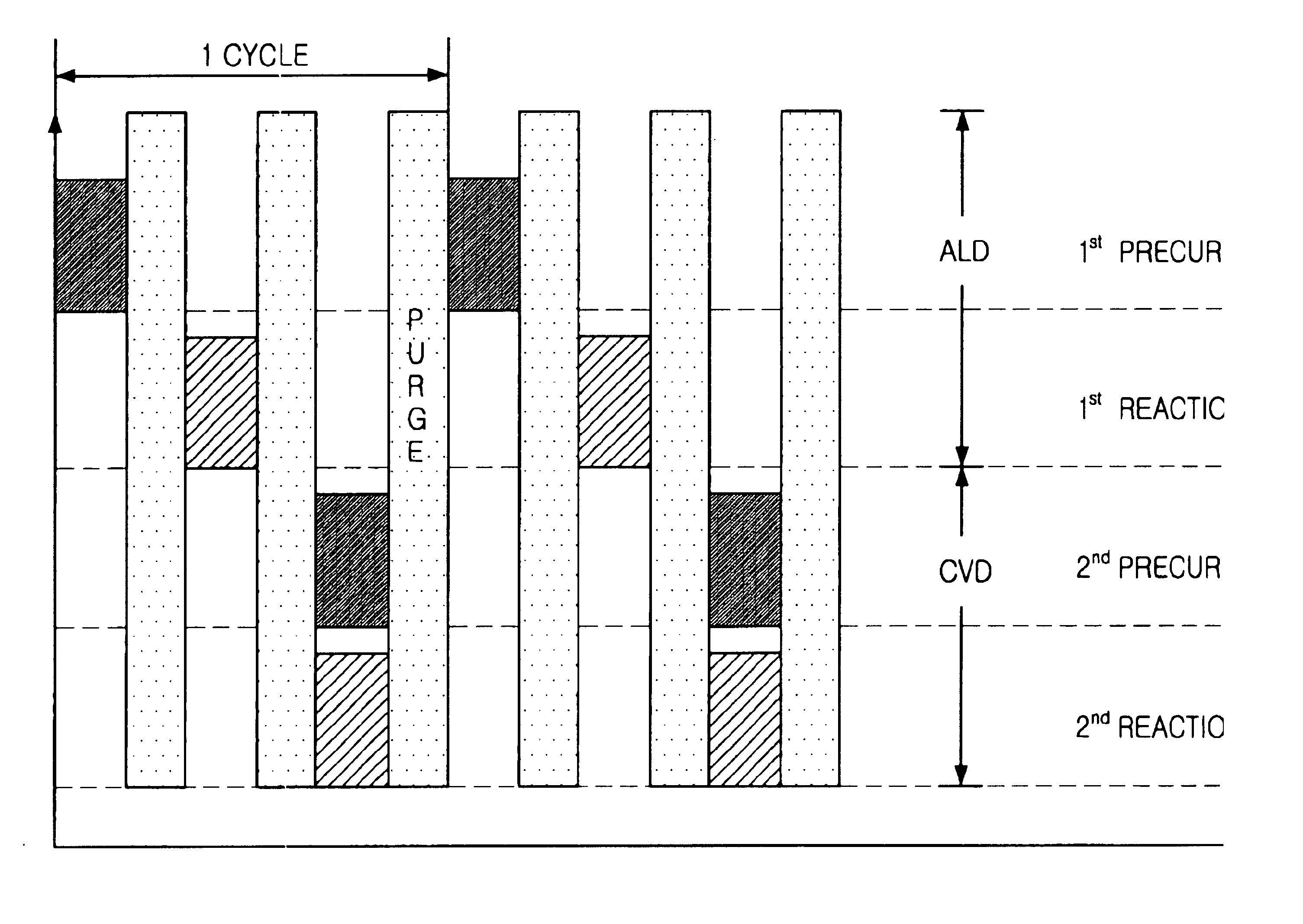
FIG. 4 shows steps of forming polyatomic layer using a mixed deposition method consisting of an atomic layer deposition method(ALD) and a chemical vapor deposition(CVD) method. Hereinafter, the method for forming BST layer will be described.

Referring to FIG. 4, a first precursor, containing a Ba source and a Sr source, is flowed into a reaction chamber and is absorbed on a substrate on which a polyatomic layer to be formed. The Ba source is selected from the group consisting of Ba(THD).sub.2 -tetraene, Ba(THD).sub.2 -triene(Ba((C.sub.11 H.sub.19 O.sub.2)--NH.sub.2 ((C.sub.2 H.sub.4)NH(C.sub.2 H.sub.4)).sub.2, Ba(THD).sub.2 -pmdt(Ba(C.sub.11 H.sub.19 O.sub.2).sub.2 --C.sub.9 H.sub.23 N.sub.3), Ba(METHD).sub.2 and Ba (O.sub.4 C.sub.14 H.sub.25).sub.2. The Sr source is selected from a group consisting of Sr(THD).sub.2 -tetraene, Sr(THD).sub.2 -triene(Sr(C.sub.11 H.sub.19 O.sub.2)--NH.sub.2 ((C.sub.2 H.sub.4)NH(C.sub.2 H.sub.4)).sub.2), Sr(THD).sub.2 -pmdt(Sr(C.sub.11 H.sub.19 O.sub.2)....


PUM

PropertyMeasurementUnit
temperatureaaaaaaaaaa

Abstract

A method for forming a polyatomic layer with a mixed deposition method consisting of an atomic layer deposition method (ALD) and a chemical vapor deposition method. The mixed deposition method can be adopted to form a polyatomic high dielectric layer, such as BST or STO. Accordingly, it is possible to form a polyatomic high dielectric layer having a uniform composition distribution, and thereby also having a high dielectric characteristic and a low leakage current characteristic.

Description

Methods for fabricating highly integrated semiconductor devices are disclosed and, more particularly, methods for forming polyatomic layers of a semiconductor device are disclosed.DESCRIPTION OF THE RELATED ARTGenerally, as semiconductor devices become highly integrated and miniaturized, the area occupied by the constitutional elements gets smaller. Although as the size of a semiconductor device shrinks, however, a minimum capacitance should be secured to drive the device.When fabricating a capacitor of a 64 Mbyte or 256 Mbyte-DRAM using a conventional dielectric material such as SiO.sub.2 or Si.sub.3 N.sub.4, the area occupied by the capacitor should be more than six times larger than the cell area to secure the essential capacitance, even though the SiO.sup.2 or Si.sub.3 N.sub.4 layer is made as thin as possible. As a planar capacitor cannot fulfill this condition, a method for increasing the charge storage area is sought.Many structures including a stack capacitor, a trench capac...

Claims


Application Information

Patent Timeline
Patent Type & Authority Patents(United States)
IPC IPC(8): H01L21/02H01L21/316H01L21/318H01L21/8242
CPCH01L21/318H01L21/31691H01L21/02271H01L21/0228H01L21/02205H01L21/02197H10B99/00
Inventor CHO, HO JIN
Owner SK HYNIX INC
Why Eureka
Try Eureka