Method and apparatus for substrate biasing in multiple electrode sputtering systems

Inactive Publication Date: 2004-11-16
ADVANCED ENERGY INDS
View PDF32 Cites 29 Cited by
  • Summary
  • Abstract
  • Description
  • Claims
  • Application Information

AI Technical Summary

Benefits of technology

It is yet another object of the present invention to provide biasing of the substrate in a dual anode or dual cathode sput

Problems solved by technology

The expelled target atoms also coat every other surface in the system, as for the most part they are neutral and there is no practical way to direct their path.
Insulators do not have free electrons available for this purpose, so that an insulating target material cannot be used.
A problem occurs in these and other cases, however, when the reaction product is an electrical insulator.
As this happens the conduction path for the electrons is coated over, and the process cannot be sustained.
This has been termed the "disappearing anode" problem.
In the past the reactive process was run until this effect began to create serious problems, whereupon the system was opened to mechanically scrub off the offending insulating layer from the anode to create a new metallic surface.
Thus, continuous operation without this maintenance was not possible.
Another drawback related to the coating of the anode with an insulator is that this insulator will generally charge up as the electrons attempt to collect there.
This charge can cause an electric field in the insulating film on the anode which may exceed the dielectric strength of the film material.
When this occurs an arc may

Method used


Image

  • Method and apparatus for substrate biasing in multiple electrode sputtering systems
  • Method and apparatus for substrate biasing in multiple electrode sputtering systems
  • Method and apparatus for substrate biasing in multiple electrode sputtering systems

Examples


Embodiment Construction

As can be easily understood, the basic concepts of the present invention may be embodied in a variety of ways. It involves both processes or methods as well as devices to accomplish such. In addition, while some specific circuitry is disclosed, it should be understood that these not only accomplish certain methods but also can be varied in a number of ways. Importantly, as to all of the foregoing, all of these facets should be understood to be encompassed by this disclosure.

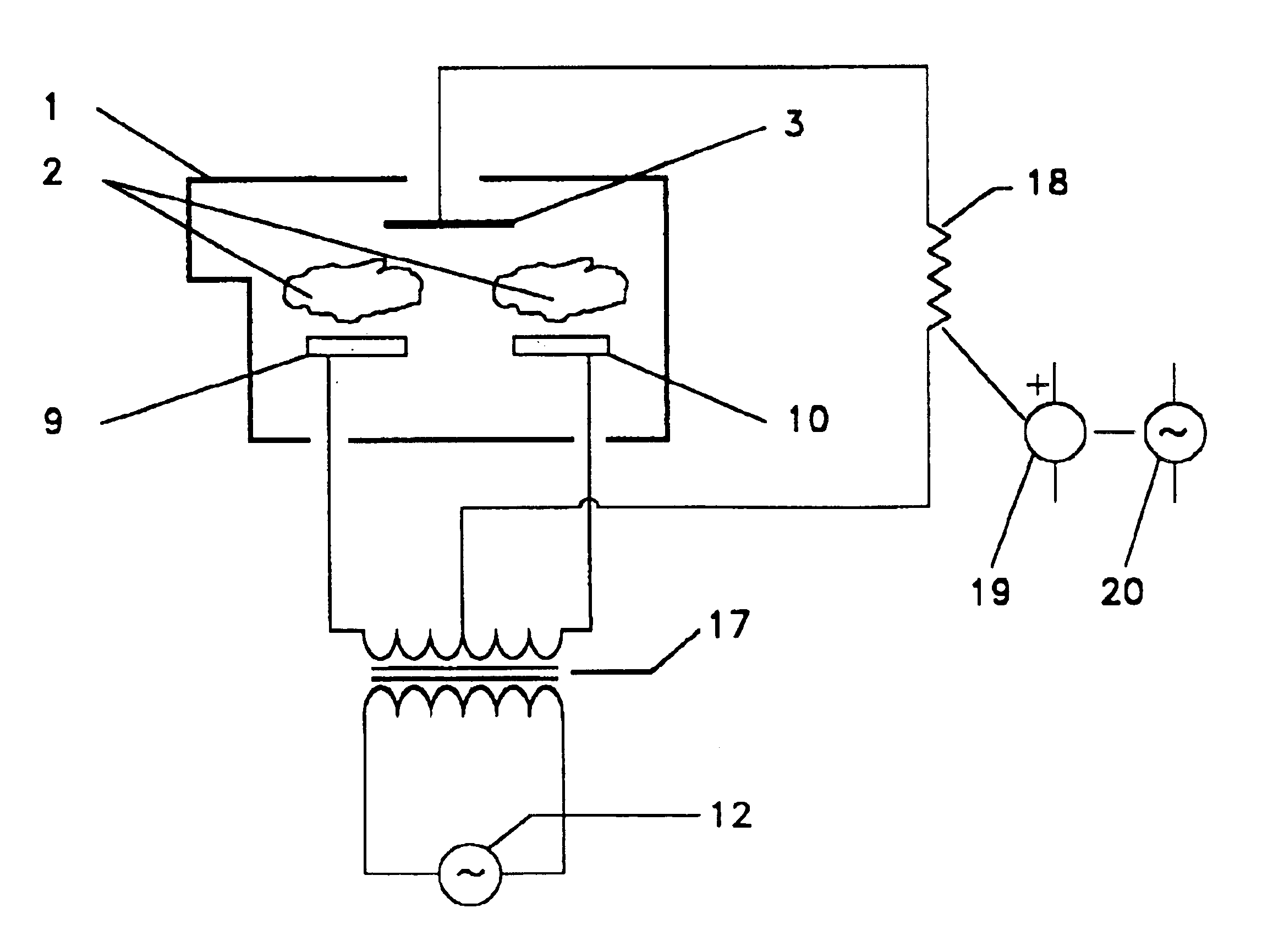
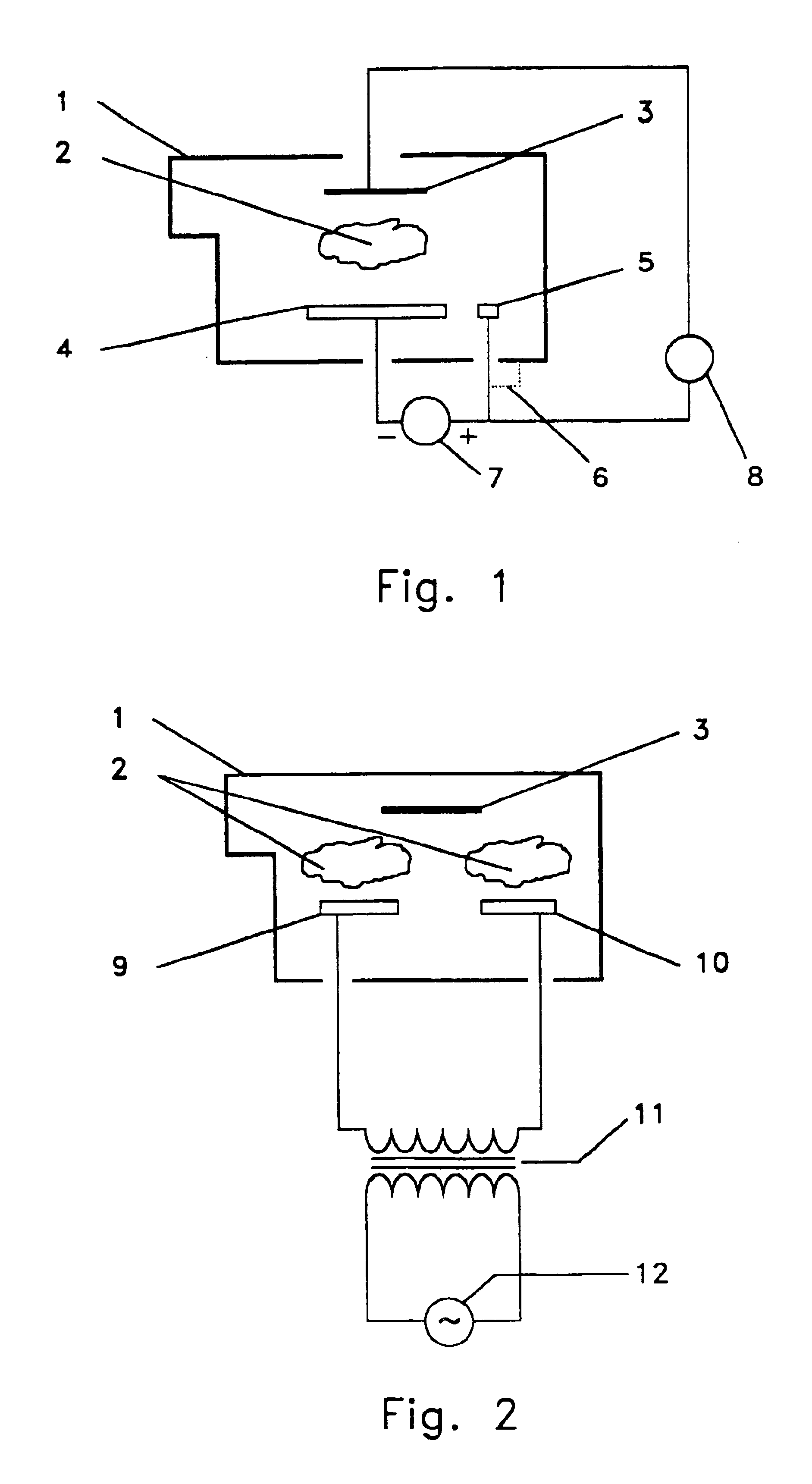
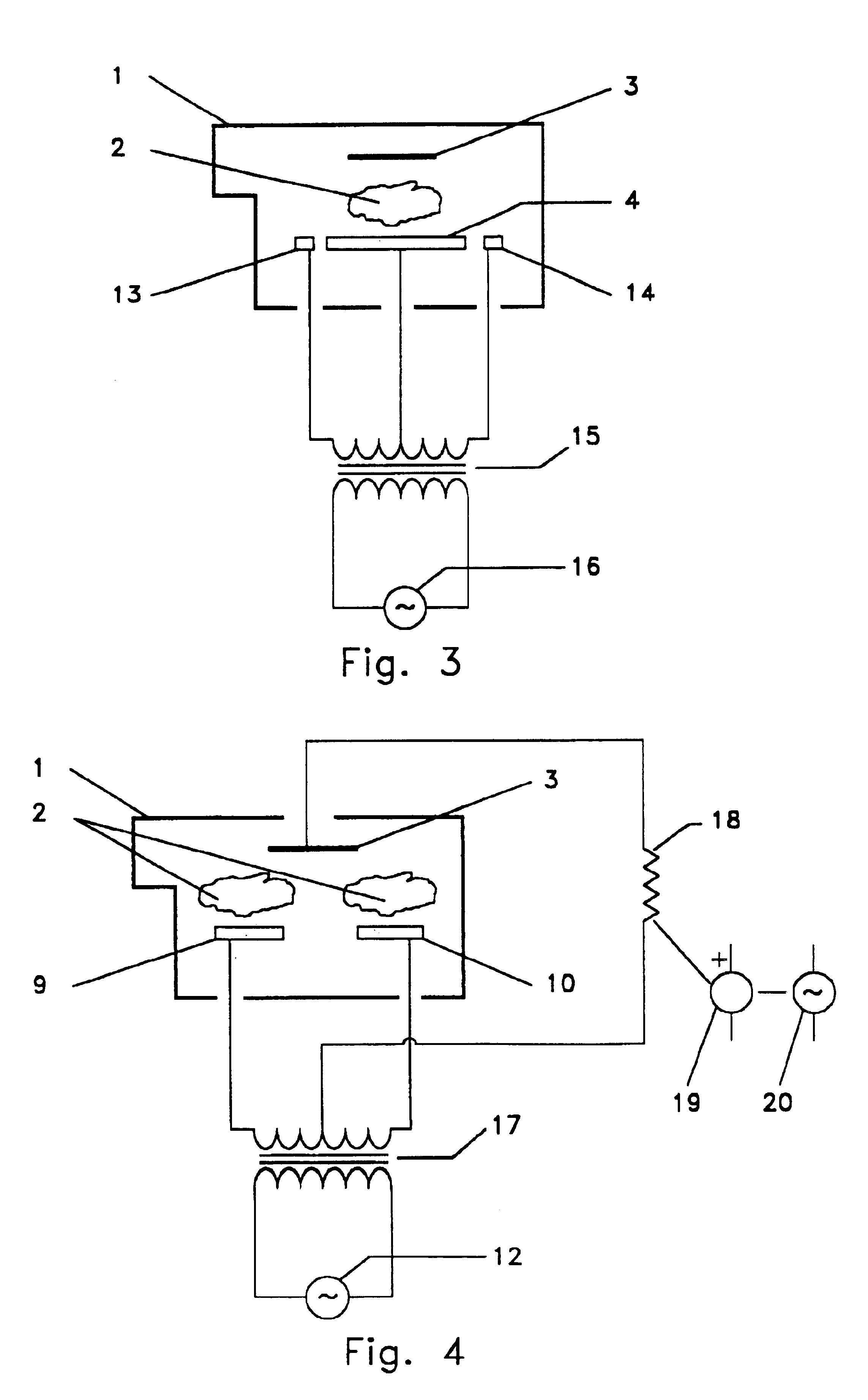
FIG. 1 shows a conventional single target system. In this case there may exist a discrete anode 5 or an alternative connection 6 may be made whereby the positive lead of sputtering power supply 7 is connected to the chamber 1 rather than to anode 5. In this case anode 5 may be dispensed with. The alternative connection 6 is shown in dotted lines in FIG. 1. Ions are attracted to target 4 from plasma 2 and upon striking target 4 cause sputtered atoms to be ejected from target 4 in accordance with well-known princip...


PUM

PropertyMeasurementUnit
Poweraaaaaaaaaa
Responsivityaaaaaaaaaa
Plasma poweraaaaaaaaaa

Abstract

A method and an apparatus are disclosed for causing ion bombardment of the substrate during sputter deposition of an insulating or conducting material on a substrate (3) when using dual cathode or dual anode sputtering approaches. A novel electrical circuit including a center-tapped transformer is disclosed to permit a controllable potential to be applied to the substrate relative to the plasma potential, without the necessity of an additional power supply. Also disclosed are approaches which permit the use of an auxiliary biasing supply (8), either dc or high frequency ac, and which can permit continuous discharging of the surface through alternate ion and electron bombardment.

Description

I. TECHNICAL FIELDThe present invention generally relates to reactive plasma sputter deposition techniques for forming and depositing films on substrates and, more particularly, is concerned with a system and method for sputter deposition of a material on a substrate using dual cathode or dual anode systems.II. BACKGROUNDSputter deposition is a process wherein a target, usually a metal, is placed in position near a plasma (a cloud of ions and electrons in equal numbers), in a chamber in which most of the air has been withdrawn. Well-known conventional means are used to create the plasma. A negative voltage is produced on the target, or cathode, relative to a separate electrode called the anode by connecting the negative lead of a dc power supply to the target. The negative voltage on the target attracts the ions from the plasma, which are accelerated toward the target. Upon arrival the collision of the ions with the target physically knocks out target atoms. These target atoms trave...

Claims


Application Information

Patent Timeline
IPC IPC(8): C23C14/34C23C14/00
CPCC23C14/0036C23C14/3464C23C14/345
Inventor SCHOLL, RICHARD A.BELKIND, ABRAHAM
Owner ADVANCED ENERGY INDS
Why Eureka
Try Eureka