Plasma display panel having an improved plane electrode structure

a technology of electrode structure and display panel, which is applied in the manufacture of electrode systems, electrode discharge tubes/lamps, and electrodes. it can solve the problems of increased heat generation of the panel, large power consumption, and large load on the drive circui

Inactive Publication Date: 2004-11-16
PIONEER CORP
View PDF26 Cites 42 Cited by
  • Summary
  • Abstract
  • Description
  • Claims
  • Application Information

AI Technical Summary

Problems solved by technology

In the conventional structure shown in FIG. 1 and FIG. 2, since the stripe plane electrode 57a is formed in a wide range over a plurality of cells, there was a problem in that the sustaining current (current that runs in accordance with the sustaining discharge), which runs in proportion to the sustaining electrode area, is too large causing large power consumption.
When the power consumption is large, it creates not only a large load on the drive circuit, but also an increase in heat generation of the panel, thus resulting in the problem of reliability.
Furthermore, the conventional structure shown in FIG. 1 and FIG. 2 tends to cause a spread of plasma into adjacent cells in vertical and horizontal directions as a result of discharge, thus creating a problem of incorrect light turn on and turn off due to discharge interferences between adjacent cells.
However, if discharge interferences can easily occur between adjacent cells, it is impossible to increase the writing voltage and the sustaining voltage because incorrect light turn on and turn off discharges occur at unselected cells adjacent to the selected cell and cause the unselected cells to turn on and turn off incorrectly when high discharges are caused by increasing the writing voltage and the sustaining voltage to high levels.
As a result, the PDP's display image quality seriously deteriorates.
On the other hand, lowering of the writing voltage and the sustaining voltage in order to suppress the discharge interferences between adjacent cells deteriorates the capability making a transition from the writing operation to the sustaining operation and makes it impossible to perform a normal luminescence display, hence also deteriorating the PDP's display image quality.
In other words, it was impossible to expand the operating margin and improve the display image quality with the conventional structure shown in FIG. 1 and FIG. 2.
First, although the conventional structure shown in FIG. 3 disclosed by the Japanese Unexamined Patent Publication No. 8-22772 of 1996 succeeds in making the plasma generated by the sustaining discharge extend thick and long thus resulting in a high luminance, it has a problem in that its sustaining electrode surface is wider so that its luminous efficiency is lower as the sustaining current is larger than the conventional structure shown in FIG. 4 disclosed by the Japanese Unexamined Patent Publication No. 8-22772 of 1996.
Next, although the conventional structure shown in FIG. 4 provides a higher luminous efficiency as the plasma generated by the sustaining discharge extends thin and long, it has a problem in that it produces less sustaining current compared to the conventional structure shown in FIG. 3, so that its luminance is lower.
The conventional structure shown in FIG. 3 has a further problem that the plasma generated by the sustaining discharge has a stronger tendency to spread in the vertical and horizontal directions than the conventional structure shown in FIG. 4, and tends to cause light to turn on and turn off incorrectly due to discharge interferences between adjacent cells.
Moreover, the conventional structures shown in FIG. 3 and FIG. 4 including the conventional structures shown in FIG. 5 and FIG. 6 disclosed in the Japanese Unexamined Patent Publication No. 8-250030 of 1996 have such reliability problems in that the Al electrodes (e.g., bus electrodes 58) get peeled off partially or totally from the transparent electrodes (e.g., plane electrodes 57b, 57c) during manufacturing processes, and the Al electrodes separate from the transparent electrodes partially or totally during the panel operation so that poor continuity occurs between them.
And disappearance of the Al electrodes and the transparent electrodes themselves due mainly to galvanic cell corrosion between them during the patterning process of the Al electrodes.
It is well known that the presence of the Al electrodes that are generally apt to produce oxides and the transparent electrodes which are essentially oxides, which contact each other, may cause various problems.
This is due to the fact that metal elements are precipitated as a result of the reduction of the transparent electrodes, which are essentially oxides, and it reduces the transmittance of the transparent electrodes and consequently their luminance.
Moreover, the boundary condition becomes sparse due to the oxidation / reduction reactions between the Al electrodes and the transparent electrodes, causing the problem of the Al electrodes that are used as the bus electrodes 58 peeling off from the transparent electrodes used as the plane electrodes 57b and 57c.
Since the bus electrodes 58 are provided to reduce the wavy dulling of the voltage pulses and to apply the specified voltage pulses to the plane electrodes 57b and 57c disposed in each cell, this is a major problem for the panel operation.
Furthermore, in the process of etching and patterning the Al electrodes using a positive type photo resist as a mask, the Al electrodes can get corroded by the organic alkali developing liquid used for developing the positive type photo resist, so that pinholes can be generated on the Al electrodes.
This phenomenon is known as a galvanic cell corrosion reaction, and it eventually causes both the Al electrodes and the transparent electrodes disappear or severely deteriorate their performances as the electrodes.
Also, the oxidation / reduction reaction caused by this potential difference as a driving force is more serious than the one caused by the heat as the driving force.

Method used


Image

  • Plasma display panel having an improved plane electrode structure
  • Plasma display panel having an improved plane electrode structure
  • Plasma display panel having an improved plane electrode structure

Examples


embodiment 1

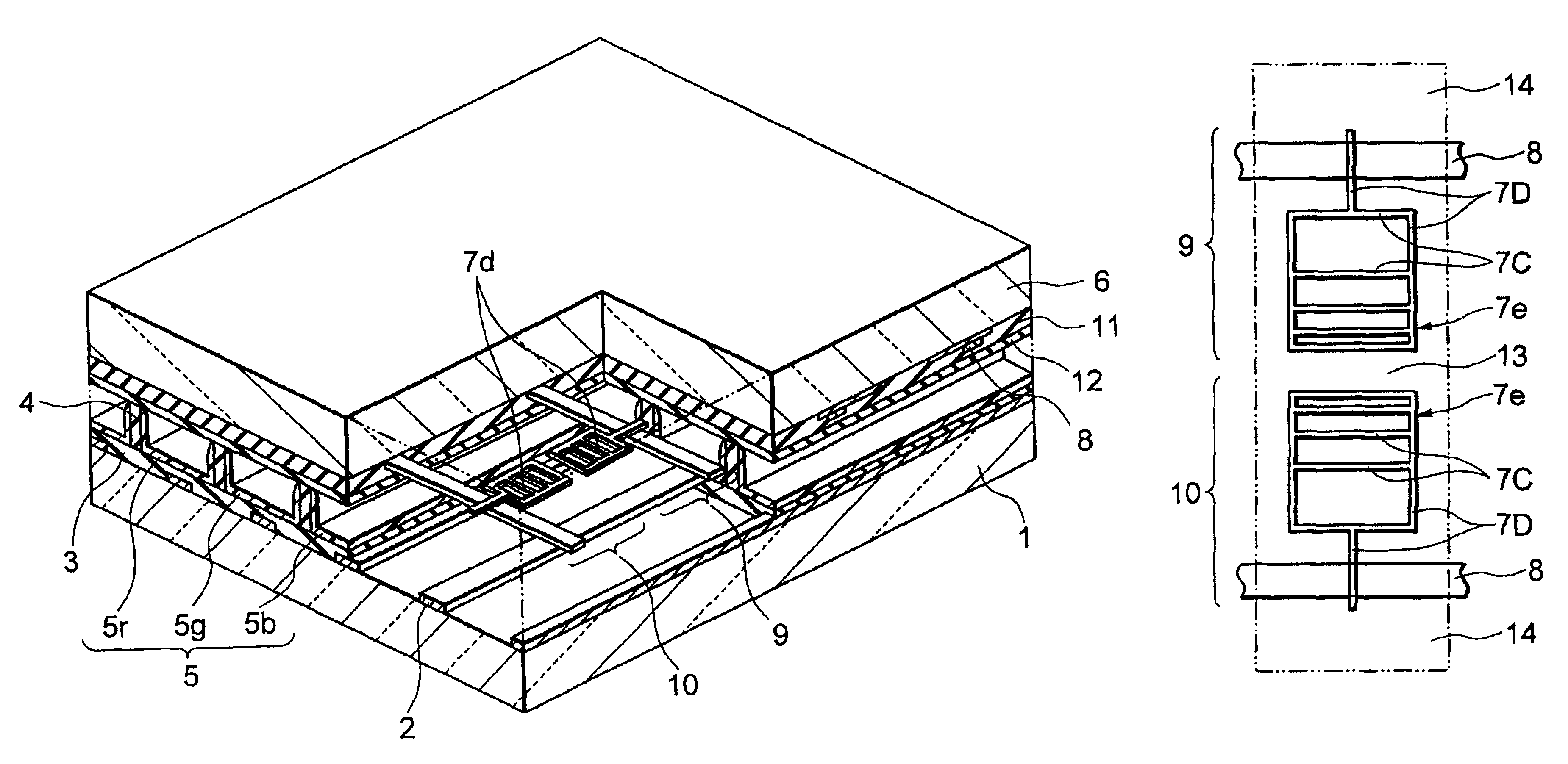
FIG. 7 is a partial cutout perspective view showing the constitution of a PDP according to a first embodiment of the present invention and FIG. 8 is a plan view showing a unit cell portion of said PDP.

In the PDP of the embodiment, a unit cell portion of the plane electrode consist of a plurality of thin wire electrodes 7A, which extend in the row direction and which are laid out at a constant interval from a discharge gap section 13 toward a non-discharge gap section 14 as shown in FIG. 8, where the left and right ends of these row direction thin wire electrodes 7A are connected with thin wire electrodes 7B that extend in the column direction to form horizontal slit-shaped plane electrodes 7d. The thin wire electrodes 7B that extend in the column direction from the center of the horizontal slit-shaped plane electrodes 7d and the bus electrodes 8 that extend in the row direction are connected to form a sustaining electrode pair (scan electrode 9 and common electrode 10).

The size of t...

embodiment 2

FIG. 11 is a plan view showing a unit cell portion of a PDP according to a second embodiment of the invention. The major difference of the second embodiment PDP in comparison with the first embodiment described above is that the plane electrodes are made into a vertical slit-shape.

More specifically, as shown in FIG. 11, a plurality of thin electrodes 7H extending in the column direction are laid out at a constant interval from the cell's vertical center axis toward the partition walls 4 and the upper and lower ends of these column direction thin wire electrodes 7H are connected by thin wire electrodes 7G that extend toward the row direction to form vertical slit-shaped plane electrodes 7g. The thin wire electrodes 7H that extend from the center of the vertical slit-shaped plane electrode 7g in the column direction and the bus electrodes 8 that extend in the row direction are connected to form a sustaining electrode pair (scan electrode 9 and common electrode 10).

The cell structure i...

embodiment 3

FIG. 14 is a plan view showing a unit cell portion of a third embodiment PDP of the invention. The major difference of the third embodiment PDP in comparison with the first embodiment described above is that the plane electrodes are made into a mesh-like shape.

More specifically, as shown in FIG. 14, a plurality of thin wire electrodes 7M extending in the row direction are laid out at a constant interval from a discharge gap section 13 toward a non-discharge gap section 14, and a plurality of thin electrodes 7N extending in the column direction are laid out at a constant interval from the cell's vertical center axis toward the partition walls 4. These row direction thin wire electrodes 7M and column direction thin wire electrodes 7N cross each other to form mesh-like plane electrodes 7j, and the thin wire electrodes 7N that extend from the center of the mesh-like plane electrodes 7j in the column direction and the bus electrodes 8 that extend in the row direction are connected to for...


PUM


Abstract

The PDP disclosed herein has a plurality of thin wire electrodes extending in the row direction, which are laid out in such a way as to widen the interval at a fixed ratio (2 times) from the discharge gap section toward the non-discharge gap section as well as to shorten the lengths of those row direction thin wire electrodes in steps with a fixed difference (approximately 20 mumxleft/right) from the cell's vertical center axis toward the partition walls. They are connected by thin wire electrodes that extend in the column direction to form antenna-shaped plane electrodes and the thin wire electrodes that extend in the column direction from the center of the antenna-shaped plane electrodes and the bus electrodes that extend in the row direction are connected to form a sustaining electrode pair (scan electrode and common electrode).

Description

1. Technical Field of the InventionThe invention relates to a plasma display panel, more specifically, to a plasma display panel having an improved plane electrode structure.2. Related ArtThe plasma display panel ("PDP") is well known as a thin flat image display device having a large display screen and displaying a mass information. In the plasma display panel, electrons are accelerated by means of an electric field to cause them to collide with a discharged gas to excite it and convert ultraviolet light irradiated through a relaxation process of the exited gas into visible light to display images. Among various types, the alternating current ("AC") PDP is superior than the direct current ("DC") PDP in terms of luminance, luminous efficiency and operating life.An example of this type of AC type PDP is disclosed in Japanese Unexamined Patent Publication No. 149873 of 1999. FIG. 1 and FIG. 2 are both plan views of a unit cell (single color illuminating cell) portion of said PDP discl...

Claims


Application Information

Patent Timeline
Patent Type & Authority Patents(United States)
IPC IPC(8): H01J17/49H01J11/12H01J11/14H01J11/22H01J11/24H01J11/26H01J11/34
CPCH01J11/12H01J11/24H01J2211/245
Inventor HIRANO, NAOTO
Owner PIONEER CORP
Why Eureka
Try Eureka