

Probe card assembly
a technology of probe card and assembly, which is applied in the direction of printed circuit assembly, non-electric welding apparatus, printed element electric connection formation, etc., can solve the problems of difficult to achieve reliable mechanical connection between free-standing resilient (spring) contact elements mounted to the terminals of space transformers, use of separate interposer components in probe card assemblies can also be undesirable, and dies are “good", so as to achieve convenient control of impedance, easy demountability, effect of effective shielding
- Summary
- Abstract
- Description
- Claims
- Application Information
AI Technical Summary
Benefits of technology
Problems solved by technology
Method used
Image

Examples
Embodiment Construction
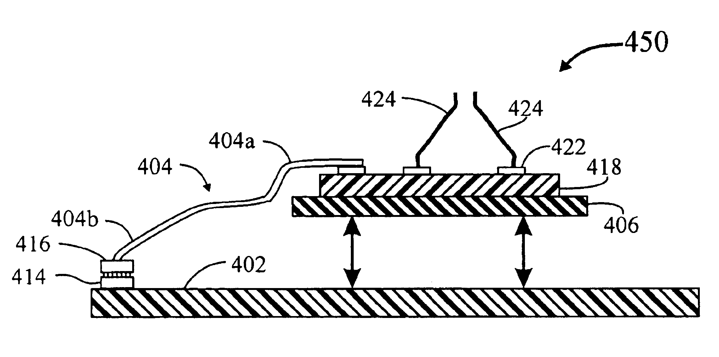
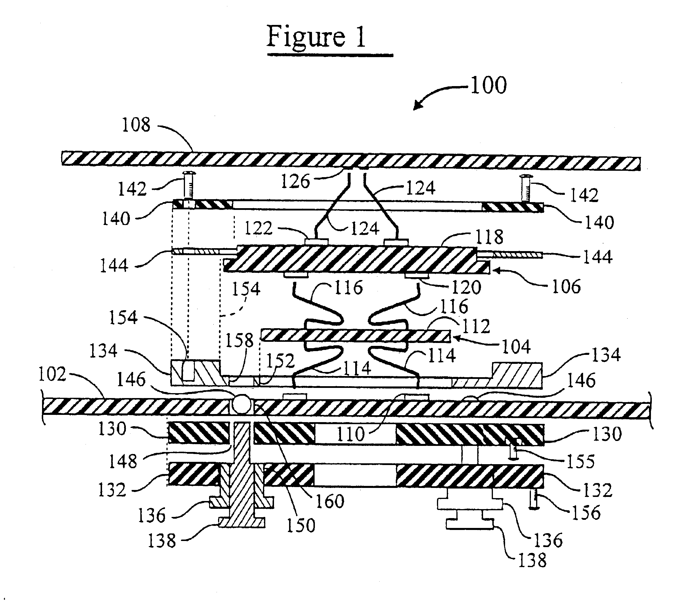
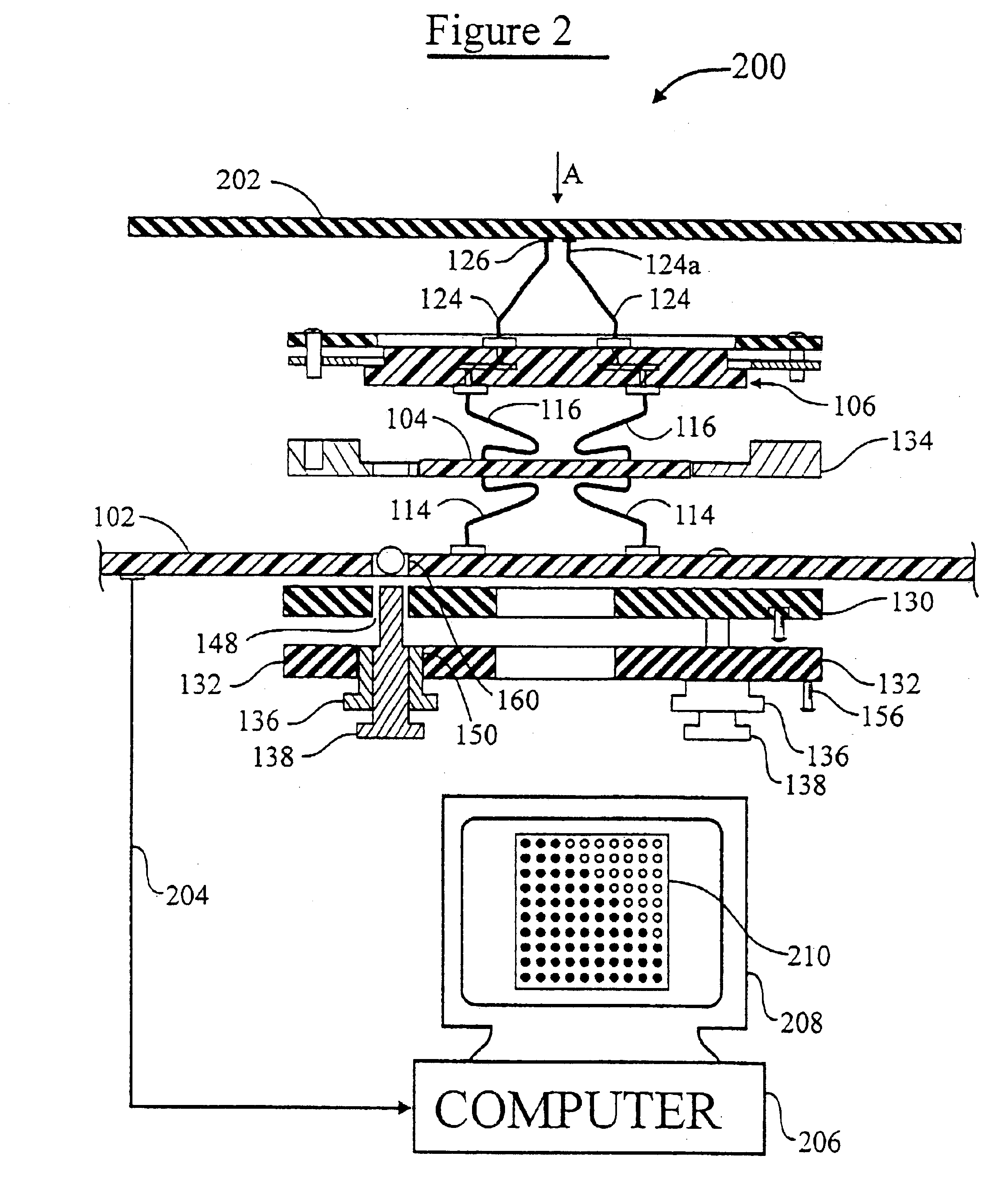
This patent application is directed to probe card assemblies, components thereof, and methods of using same. As will be evident from the description that follows, the use of resilient (spring) contact structures to effect pressure connections to terminals of an electronic component is essential. The resilient contact structures are suitably (but not necessarily) implemented as “composite interconnection elements”, such as have been described in the disclosure of the aforementioned U.S. patent application Ser. No. 08 / 452,255 (“PARENT CASE”), incorporated by reference herein.
According to an aspect of the invention, the probe elements (resilient contact structures extending from the top surface of the space transformer component) are preferably formed as “composite interconnection elements” which are fabricated directly upon the terminals of the space transformer component of the probe card assembly. The “composite” (multilayer) interconnection element is fabricated by mounting an elon...
PUM
| Property | Measurement | Unit |
|---|---|---|
| length | aaaaa | aaaaa |
| length | aaaaa | aaaaa |
| diameter | aaaaa | aaaaa |
Abstract
Description
Claims
Application Information