3-D spiral stacked inductor on semiconductor material

Inactive Publication Date: 2005-01-11
CHARTERED SEMICONDUCTOR MANUFACTURING
View PDF5 Cites 39 Cited by
  • Summary
  • Abstract
  • Description
  • Claims
  • Application Information

AI Technical Summary

Benefits of technology

The present invention provides a 3-D spiral inductor having a substrate with a plurality of turns in a plurality of levels wherein the number of levels increases from an inner turn to the outer turns of the inductor. First and second connecting portions are respectively connected to an inne

Problems solved by technology

However, despite efforts by many researchers having skill in the art, achieving high performance on-chip inductors, i.e., high qualify factor (Q), still remains a major problem especially when radio frequency integrated circuits (RFICs) are built on silicon.
Spiral inductors fabricated on such a lossy substrate suffer from high capacitive and magnetic losses.
In addition, high dynamic resistance of metal lines at GHz frequency ranges further degrades the inductor performance in CMOS technology as compared to those fabricated in monolithic microwave integrated circuits (MMICs).
Despite achieving good results, industries are reluctant to adopt such a technique because of reliability issues such as packaging yield, as well as long-term mechanical stability.
This technique has yielded significant results, however, the substrate becomes unsuitable for building active MOS devices.
The most critical factor hindering the performance of silicon-based inductors is the high resistive aluminum-copper (AlCu) interconnects used in silicon processes.
However, such approach suffers from high power consumption and high

Method used


Image

  • 3-D spiral stacked inductor on semiconductor material
  • 3-D spiral stacked inductor on semiconductor material
  • 3-D spiral stacked inductor on semiconductor material

Examples


Example

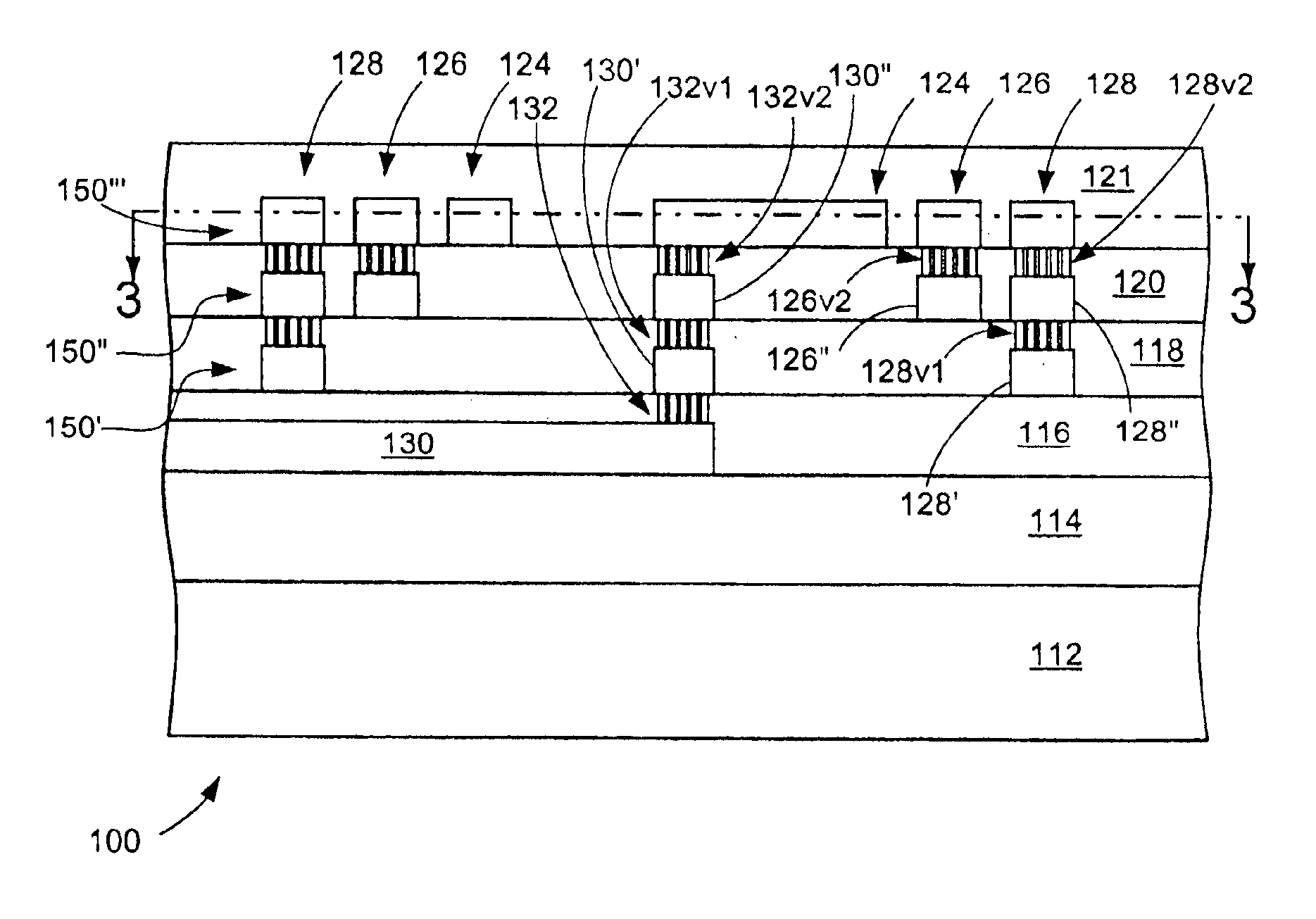
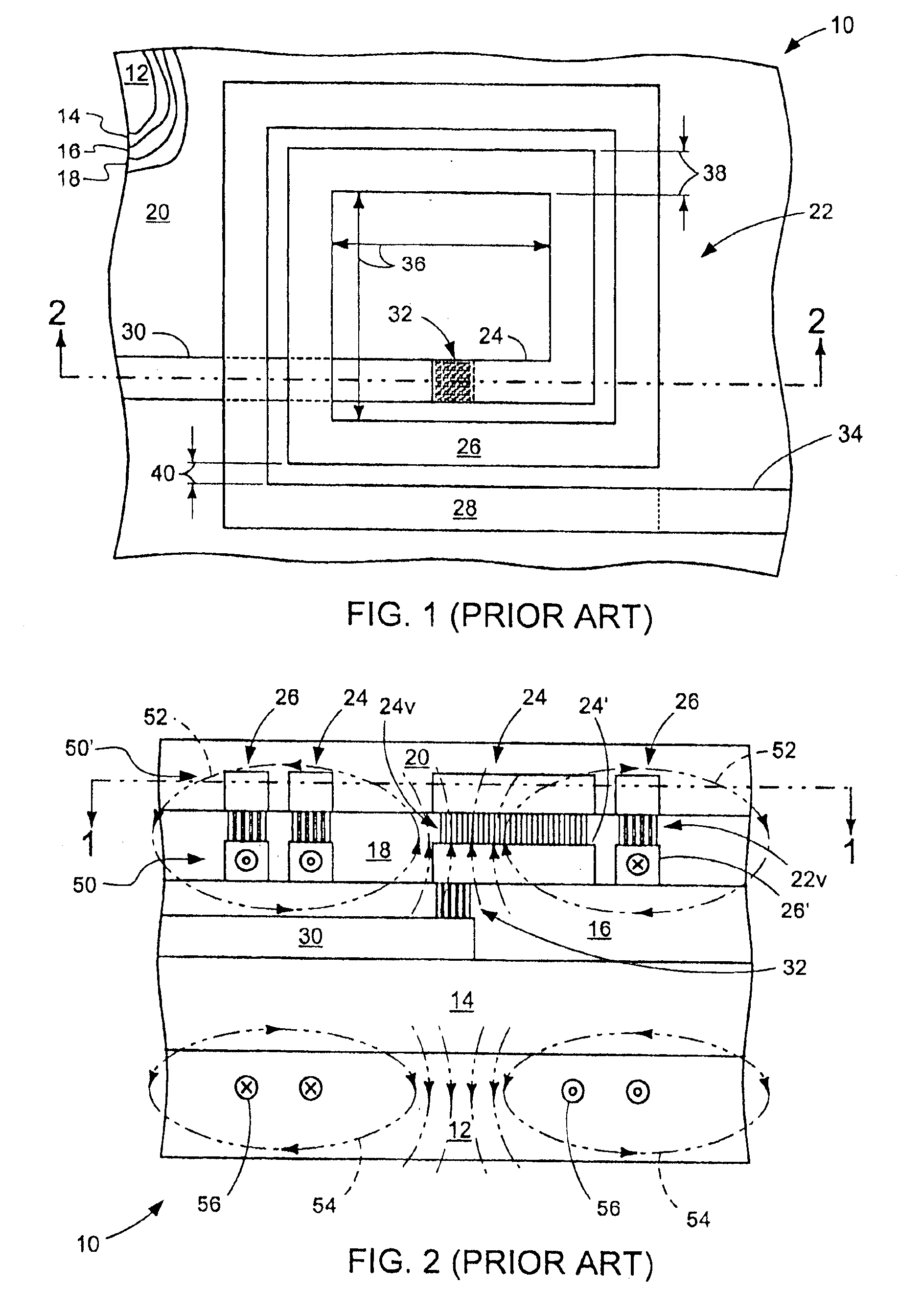
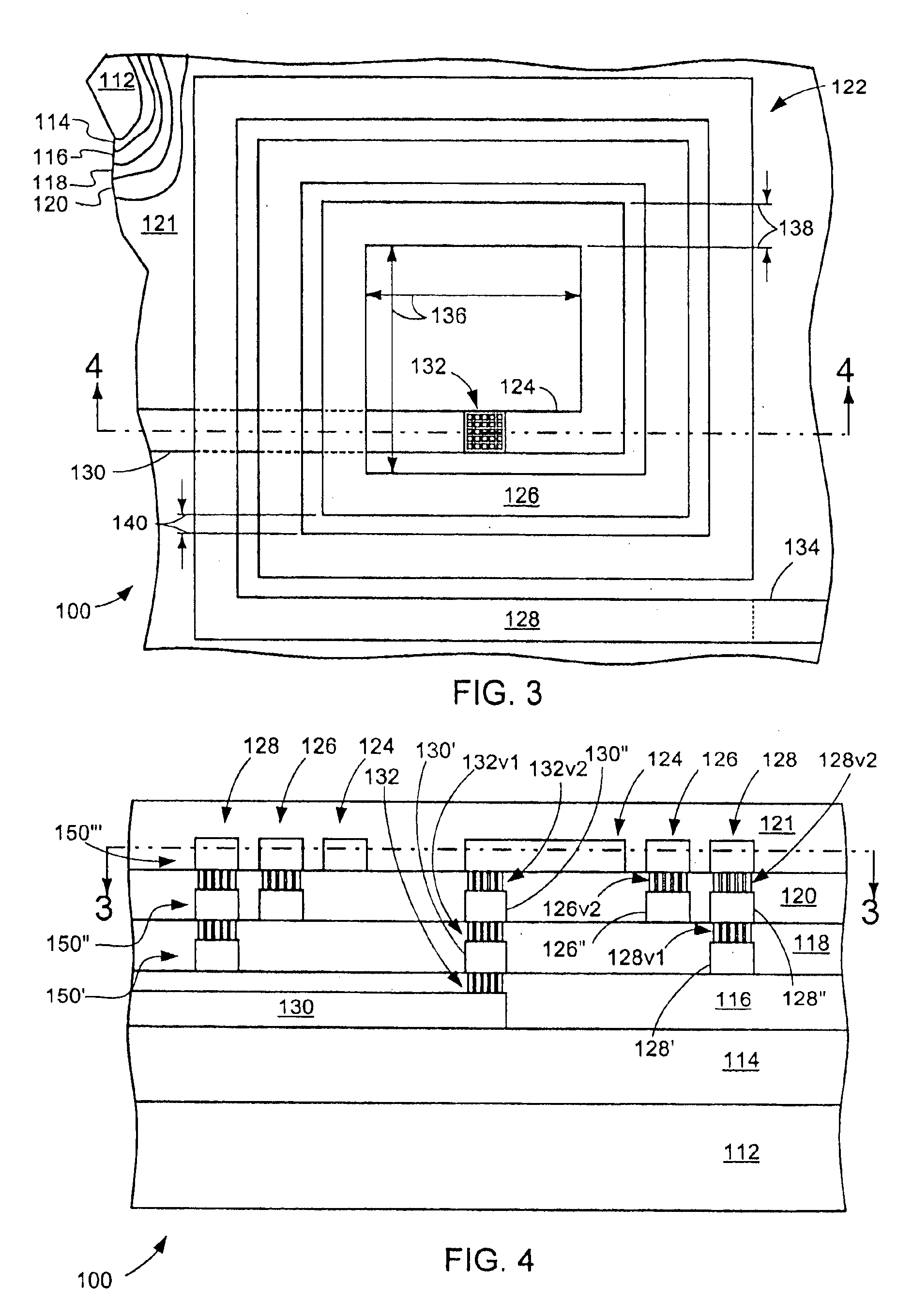
Referring now to FIG. 1 (PRIOR ART), therein is shown a cross-sectional view of a prior art on-chip inductor 10 along line 1—1 of FIG. 2 (PRIOR ART). A substrate 12, of a material such as silicon, has a plurality of dielectric layers formed thereon of a material such as silicon dioxide. Sequentially, a field dielectric layer 14 (such as a field oxide), a connecting interlayer dielectric (ILD) layer 16 (such as a silicon oxide), a first level ILD layer 18, and a second level ILD layer 20 are formed over the substrate 12. Embedded within the dielectric layers is a spiral stacked inductor 22.

The term “over” as used in herein is defined vertically above a horizontal plane parallel to the conventional surface of a wafer on which the on-chip inductor is formed regardless of the orientation of the wafer. Terms, such as “on”, “below”, “higher”, “lower”, “above”, and “under”, are defined with respect to the horizontal plane.

The term “processed” or “forming” as used herein to refer to the for...


PUM

PropertyMeasurementUnit
Lengthaaaaaaaaaa

Abstract

A 3-D spiral stacked inductor is provided having a substrate with a plurality of turns in a plurality of levels wherein the number of levels increases from an inner turn to the outer turn of the inductor. First and second connecting portions are respectively connected to an inner turn and an outermost turn, and dielectric material contains the first and second connecting portions and the plurality of turns over the substrate.

Description

TECHNICAL FIELDThe present invention relates generally to integrated circuits and more particularly to on-chip silicon-based inductors.BACKGROUND OF THE INVENTIONIncreasing demands for personal mobile communications equipment have motivated recent research activities to focus on the development of inexpensive, small size, low power consumption, and low noise level systems. To satisfy these requirements, one of the most important and indispensable circuit components is the on-chip silicon-based inductor.As a result, miniaturization of the inductor on silicon has become a current key research area and extensive work has been done in this area. However, despite efforts by many researchers having skill in the art, achieving high performance on-chip inductors, i.e., high qualify factor (Q), still remains a major problem especially when radio frequency integrated circuits (RFICs) are built on silicon.Conventional inductors built on silicon are generally planar in nature. The current compl...

Claims


Application Information

Patent Timeline
IPC IPC(8): H01L27/08H01F17/00H01F41/04H01L21/02
CPCH01L27/08H01L28/10Y10T29/4902Y10T29/4906Y10T29/49073Y10T29/49165
Inventor SIA, CHOON-BENGYEO, KIAT SENGCHU, SHAO-FU SANFORDNG, CHENG YEOWCHEW, KOK WAIGOH, WANG LING
Owner CHARTERED SEMICONDUCTOR MANUFACTURING
Why Eureka
Try Eureka