
Exposure apparatus and exposure method using same

a technology of exposure apparatus and exposure method, which is applied in the field of exposure apparatus, can solve the problems of serious degradation of detection accuracy, significant problems in fabricating a half-mirror, and the inability to assemble an optical system using lenses to form an appropriate projection exposure apparatus

Inactive Publication Date: 2005-01-11
NIKON CORP
View PDF6 Cites 35 Cited by
  • Summary
  • Abstract
  • Description
  • Claims
  • Application Information

AI Technical Summary

Benefits of technology

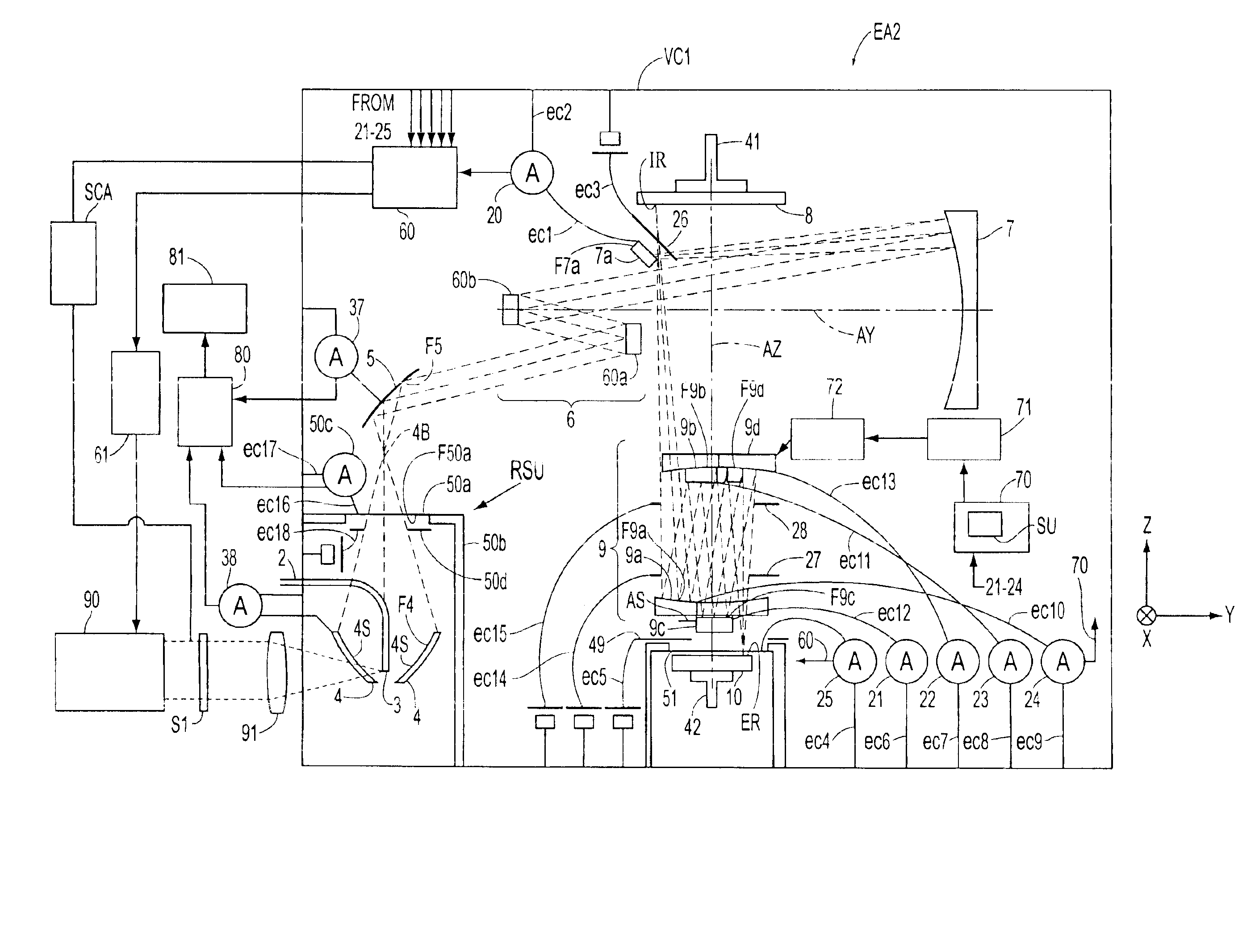
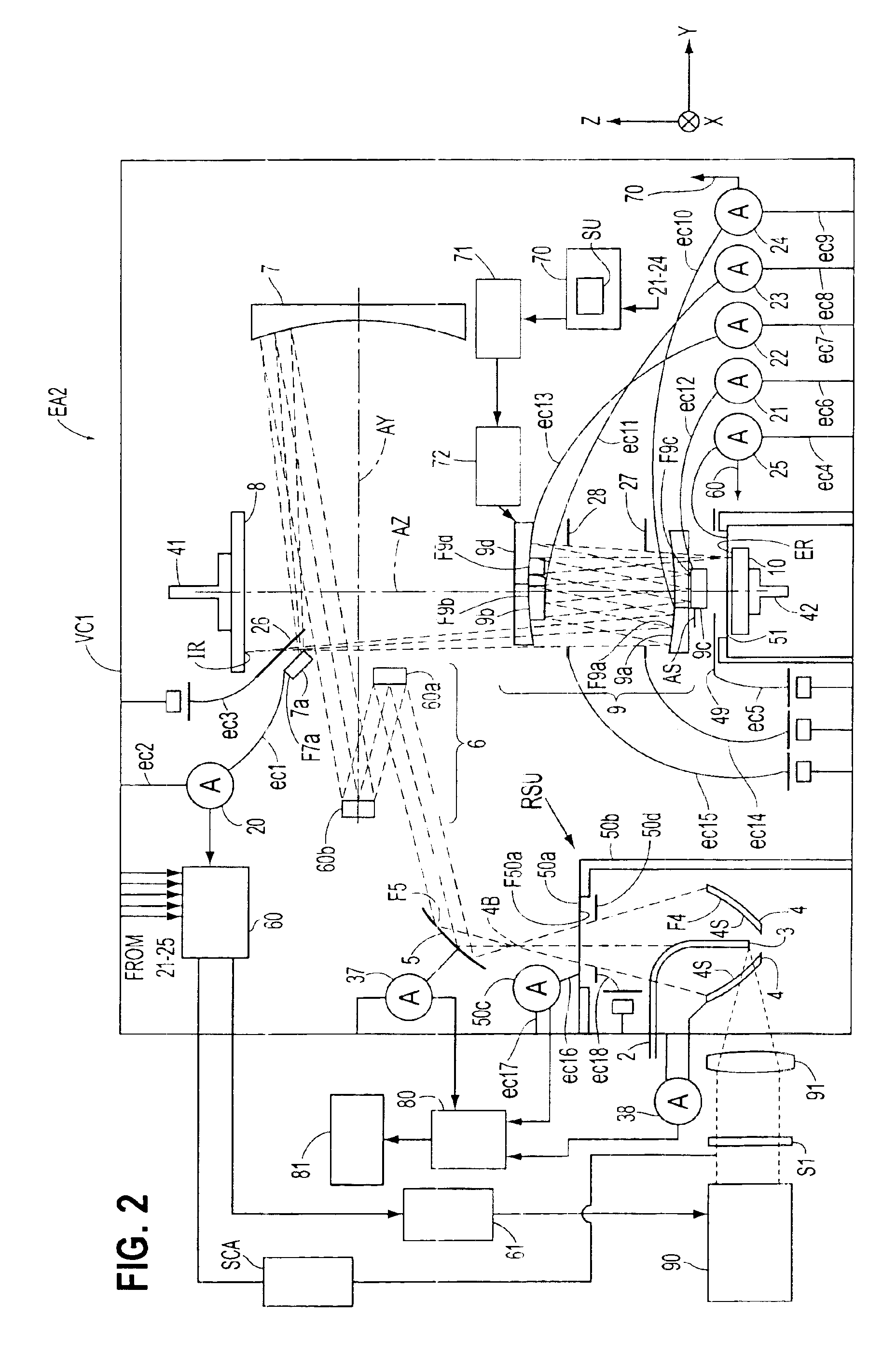
It is a goal of the present invention, in view of the above problem, to provide, without using an optical member like a half mirror that amplitude-divides a light or radiation beam, an exposure apparatus and method that can detect the intensity of exposure of radiation having a wavelength in the soft X-ray region, that can perform various measurements on the same and thereby control the timing and intensity of illumination, i.e. the exposure dose, during a photolithographic process.

Problems solved by technology

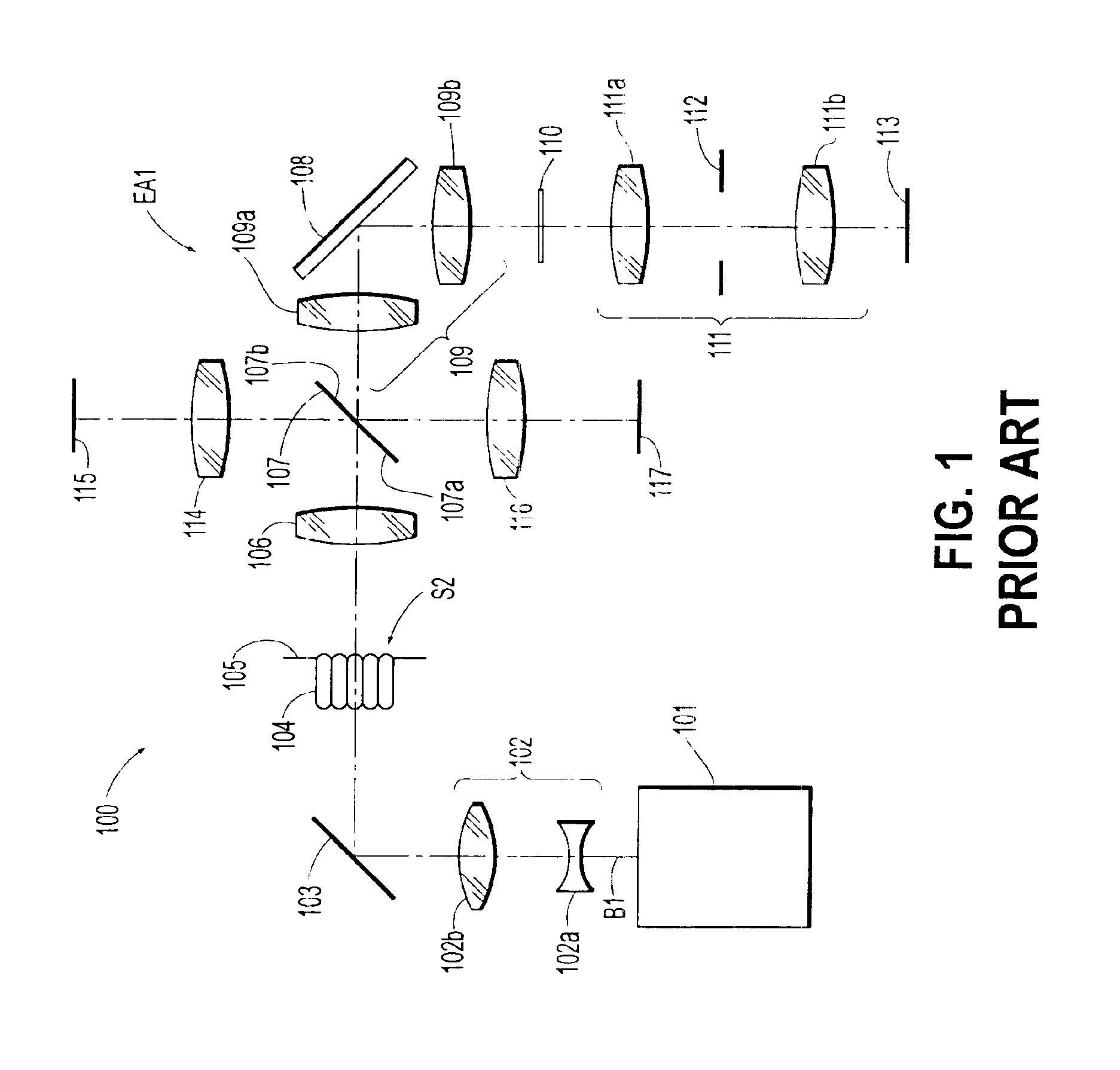
Thus, it is impossible to assemble an optical system using lenses to form an appropriate projection exposure apparatus.
Alternatively, if the exposure light beam is wavefront-divided using an optical member that wavefront-divides the exposure light-beam in place of a half mirror, a serious degradation in detection accuracy occurs.
However, significant problems exist in fabricating a half mirror that can amplitude-divide electromagnetic radiation beam having a wavelength in the soft X-ray region.

Method used


Image

  • Exposure apparatus and exposure method using same
  • Exposure apparatus and exposure method using same
  • Exposure apparatus and exposure method using same

Examples


Embodiment Construction

The present invention relates to exposure apparatus that uses X-rays during a photolithographic process in the fabrication of semiconductor devices with high levels of integration, and more particularly such apparatus that uses soft X-rays and an exposure control method using same.

If a material surface is irradiated with radiation, electrons are ejected from the surface due to the photoelectric effect. When this occurs, the maximum kinetic energy EMAX of the electrons is expressed by condition (2) below:

EMAX=hv−w  (2)

Therein, h is Planck's constant, v is the frequency of the radiation, and w is a work function.

The photoelectric effect in condition (2) above is produced under the condition of hv>w. However, if the material surface that produces the photoelectric effect is metal, then work function w is several electron-volts, which is equivalent to several hundred nanometers when converted to a wavelength.

Accordingly, the photoelectric effect can be reliably obtained even with radia...


PUM


Abstract

An exposure apparatus (EA2) that uses X-ray radiation in a photolithographic process and can obtain various measurements regarding the X-ray radiation used, by obtaining and analyzing readings of the photoelectric effect on various reflective surfaces (5, 60a, 60b, 7, 7a, 9a, 9b, 9c and 9d) or optical elements (50a and 51). With the measurements of the X-ray radiation, the exposure apparatus can control the exposure dose during the mask (8) and wafer (10) illumination process. The exposure system also has the ability to detect deformation in the mirrors (9a, 9b, 9c and 9d) of the projection optical system caused by heat generated by absorption of the X-ray radiation. This is accomplished by analyzing the photoelectric effect occurring on the mirror surfaces and correcting the deformation of the mirrors based on this analysis.

Description

FIELD OF INVENTIONThe present invention relates to exposure apparatus that uses X-rays during a photolithographic process in the fabrication of semiconductor devices with high levels of integration, and more particularly such apparatus that uses soft X-rays and an exposure control method using same.BACKGROUND OF THE INVENTIONTo accurately and faithfully transfer or project a fine pattern of a mask onto a photosensitive substrate (wafer) with an exposure apparatus for manufacturing semiconductor devices by photolithography, it is essential to extract a portion of the exposure light (radiation) in the optical path between the light source that supplies the exposure light and the photosensitive substrate, and to perform various measurements on the extracted light.In a conventional exposure apparatus, a light-dividing member such as a half mirror is positioned in the optical path between the light source and the photosensitive substrate. The light-dividing member then extracts a portion...

Claims


Application Information

Patent Timeline
IPC IPC(8): G03F7/20G02B17/00H01L21/027
CPCG03F7/70058G03F7/70233G03F7/70916G03F7/70591G03F7/7085G03F7/70558
Inventor KOMATSUDA, HIDEKIKONDO, HIROYUKI
Owner NIKON CORP
Learn More