Method of manufacturing a semiconductor device and manufacturing system

a manufacturing system and semiconductor technology, applied in the direction of total factory control, programme control, electric programme control, etc., can solve the problem that the process conditions may fall into a slack range, and achieve the effect of improving throughput and yield

Inactive Publication Date: 2005-01-11
HITACHI LTD
View PDF10 Cites 41 Cited by
  • Summary
  • Abstract
  • Description
  • Claims
  • Application Information

AI Technical Summary

Benefits of technology

The present invention has been made in view of the above circumstances and has an object to overcome the above problems and to provide a method of manufacturing semiconductor devices and a manufacturing system for the same, which

Problems solved by technology

It is needless to say that the process conditions may fall into a slack ra

Method used


Image

  • Method of manufacturing a semiconductor device and manufacturing system
  • Method of manufacturing a semiconductor device and manufacturing system
  • Method of manufacturing a semiconductor device and manufacturing system

Examples


first embodiment

[First Embodiment]

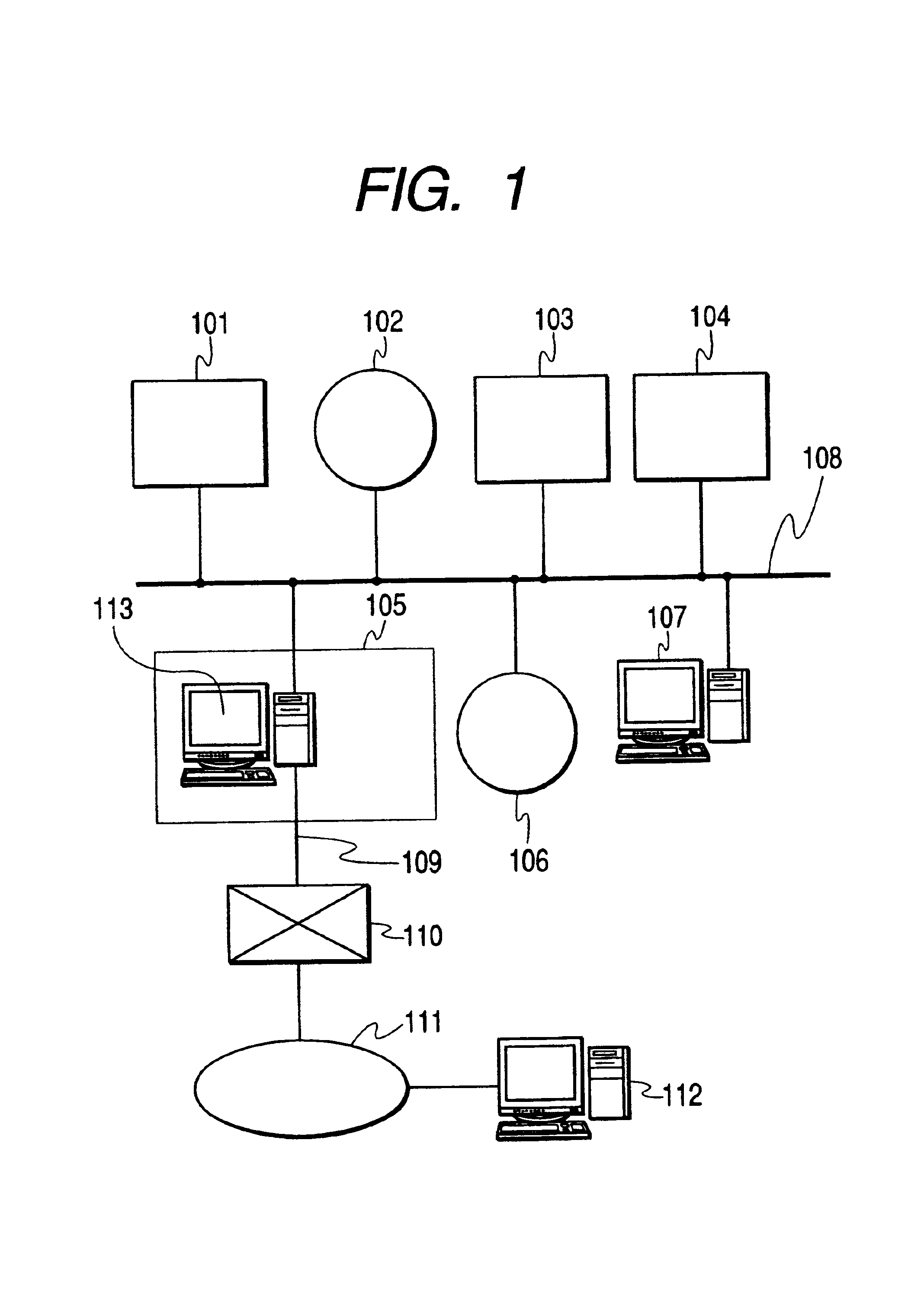
A first preferred embodiment will be described in greater details herein below by referring to FIG. 1, which shows part of a production line of semiconductor devices in accordance with the present invention for use with a network.

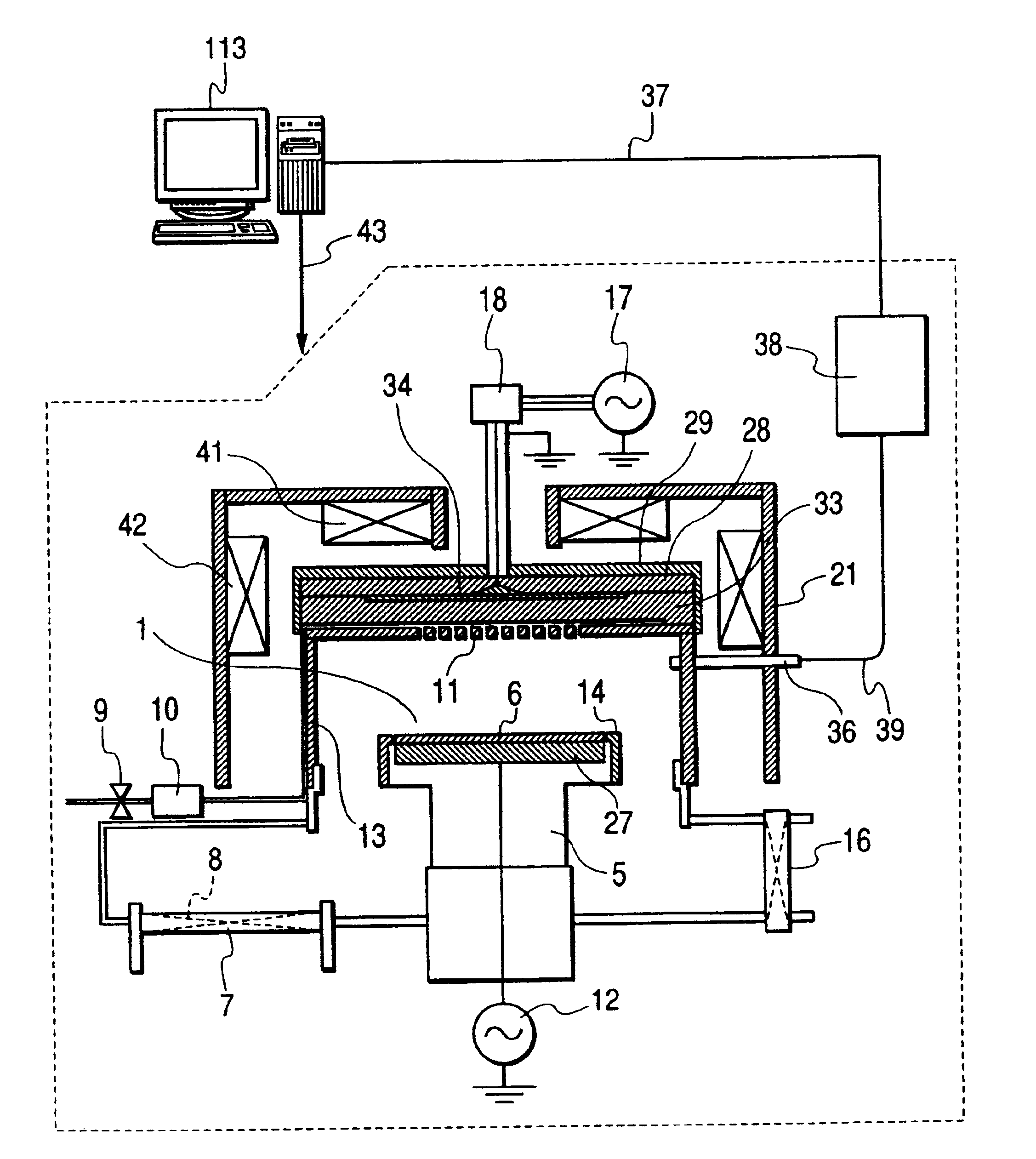
The processing wafer will be carried on a transporter robot and transported from polysilicon deposition equipment 101, through SiO2 layer deposition equipment 103, exposure and development equipment 104 to etching equipment 105. The etching equipment 105 has an oxide processing unit as shown in FIG. 2, and a gate processing unit as shown in FIG. 3. The etching equipment 105 also has one washing chamber and a computer 113 for controlling the equipment.

A washing process is installed after the deposition equipment and the etching equipment. Some wafers will be transported to the thickness interferometer 102 and to the scanning electron microscope 106 for the inspection. The information on masks (such as the surface area subject to be etched, ...

second embodiment

[Second Embodiment]

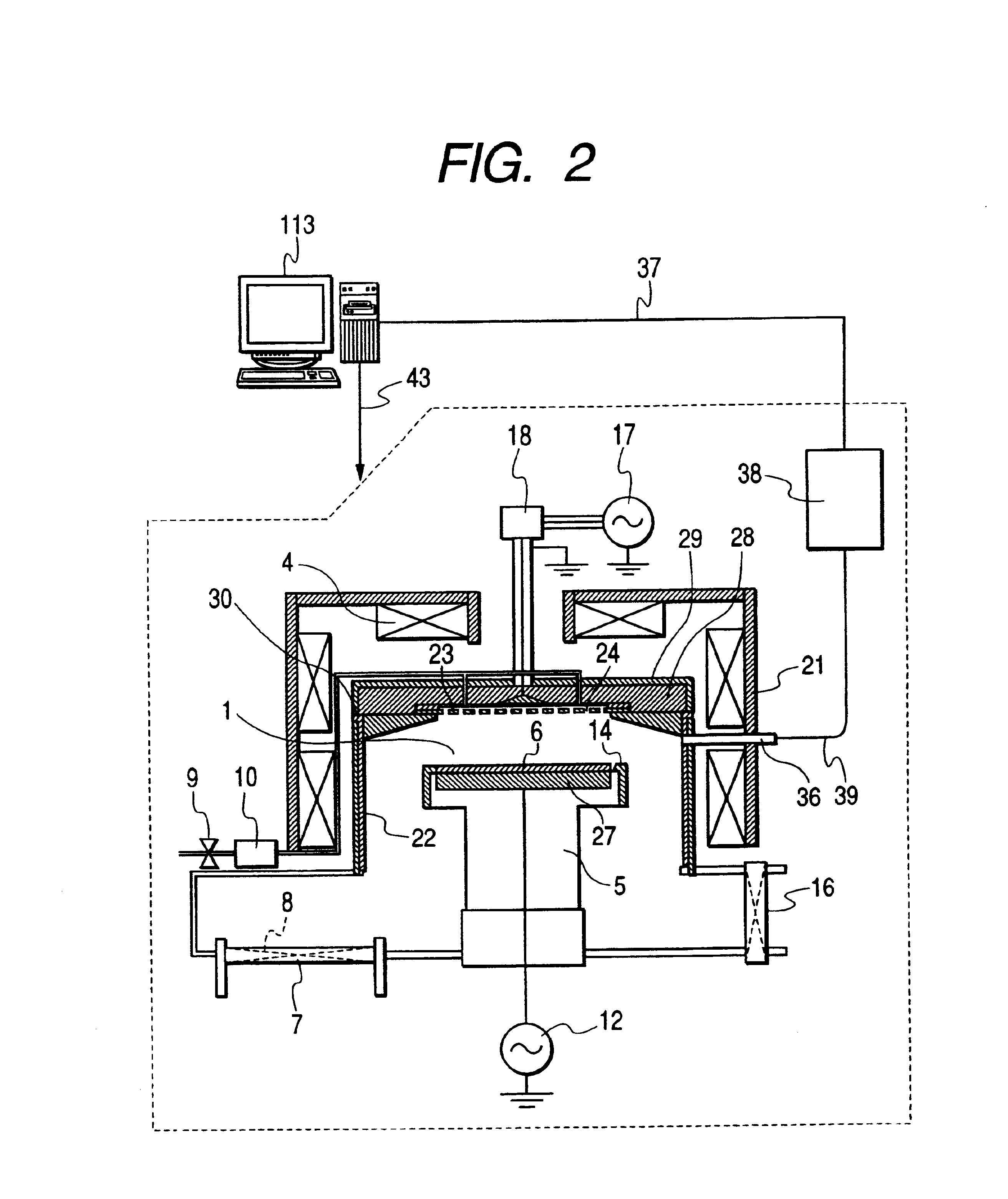
Another preferred embodiment using the architecture shown in FIG. 6 in accordance with the present invention will be described in greater details herein below. In FIG. 6, part of a mass production line of semiconductor devices is shown. The wafer to be processed will be carried on a transporter robot and transported through silicone oxide deposition equipment 401, and exposure and development equipment 104 to etching equipment 402. In the etching equipment 402 an oxide processing unit shown in FIG. 2 is provided, associated with one ashing chamber and a computer 113 for controlling the equipment. After the deposition and etching, wafer will be transferred to the lavage. Part of wafers in a lot will be separately transferred to the thickness interferometer 102 and to the scanning electron microscope 106 for the inspection. The information on the mask (such as the surface area subject to be etched, thickness of oxide layer, thickness of mask, kinds of oxide, critica...

third embodiment

[Third Embodiment]

Yet another preferred embodiment of the present invention will be described in greater details with reference to the equipment shown in FIG. 11. The equipment shown in FIG. 11 includes etching chambers 901 and 902, a transport chamber 903, as well as a detector 905 associated with it. The etching chambers has the structure shown in FIG. 3. The detector emits slantwise light beams to the wafer surface and detects the intensity of reflected beam to determine the surface area to be etched. In the computer 113 of the etching equipment many deposition conditions that include input items with respect to the wafers having been processed and the etching conditions are stored and linked together. There is provided a database developed by the vendor in the computer, which database stores certain data including the surface area to be etched, amount of dosage, and annealing temperature. The database also contains the dependent data such as the gas flow rate, and gas pressure w...


PUM


Abstract

Automatic generation of processing conditions will be provided, based on a database and process modeling by a computer equipped in semiconductor device fabrication equipment, by using input of wafer processing history including the thickness and quality. The computer equipped in semiconductor device fabrication equipment obtains the wafer processing and inspection results from a production line management computer in order to assist input of the process history. The computer in the fabrication equipment can be connected to computers in a fabrication equipment manufacturer on a communication network to automatically provide process conditions and maintenance schedule.

Description

BACKGROUND OF THE INVENTION1. Field of the InventionThe present invention relates to a method of manufacturing a semiconductor device and manufacturing system.2. Description of the Prior ArtSemiconductor devices are produced by the fabrication process in combination of ion implantation, film deposition by means of sputtering equipment or CVD (chemical vapor deposition) equipment, transcription for delineating a mask pattern on a resist mask by exposing and developing, thin film process by etch, and washing / rinse. Each semiconductor device manufacturing equipment is handled as a separate machine. The process conditions in each equipment have been optimized for that single equipment, in most cases. More specifically, each of process engineers decides such process conditions as kind of feeding gas, gas flow rate, gas pressure, output power of high frequency waves, processing time, processing temperature, processing stage position, and the like on the basis of wafer process information ...

Claims


Application Information

Patent Timeline
IPC IPC(8): H01L21/00G05B19/418H01L21/302H01L21/02H01L21/3065
CPCG05B19/41875H01L21/67276G05B2219/31288G05B2219/32198G05B2219/45031G05B2219/32053Y02P90/02Y02P90/80H01L21/02
Inventor IZAWA, MASARUMORI, MASAHITONEGISHI, NOBUYUKITACHI, SHINICHI
Owner HITACHI LTD
Why Eureka
Try Eureka