

Multiple-gate transistors with improved gate control
a multi-gate transistor and gate control technology, which is applied in the direction of transistors, semiconductor devices, electrical equipment, etc., can solve the problems of inability to substantially control the on and off of the transistor, the requirement for body-doping concentration, the thickness of the gate oxide, and the difficulty of meeting the source/drain (s/d) doping profiles, etc., to achieve high permittivity
- Summary
- Abstract
- Description
- Claims
- Application Information
AI Technical Summary
Benefits of technology
Problems solved by technology
Method used
Image

Examples
Embodiment Construction
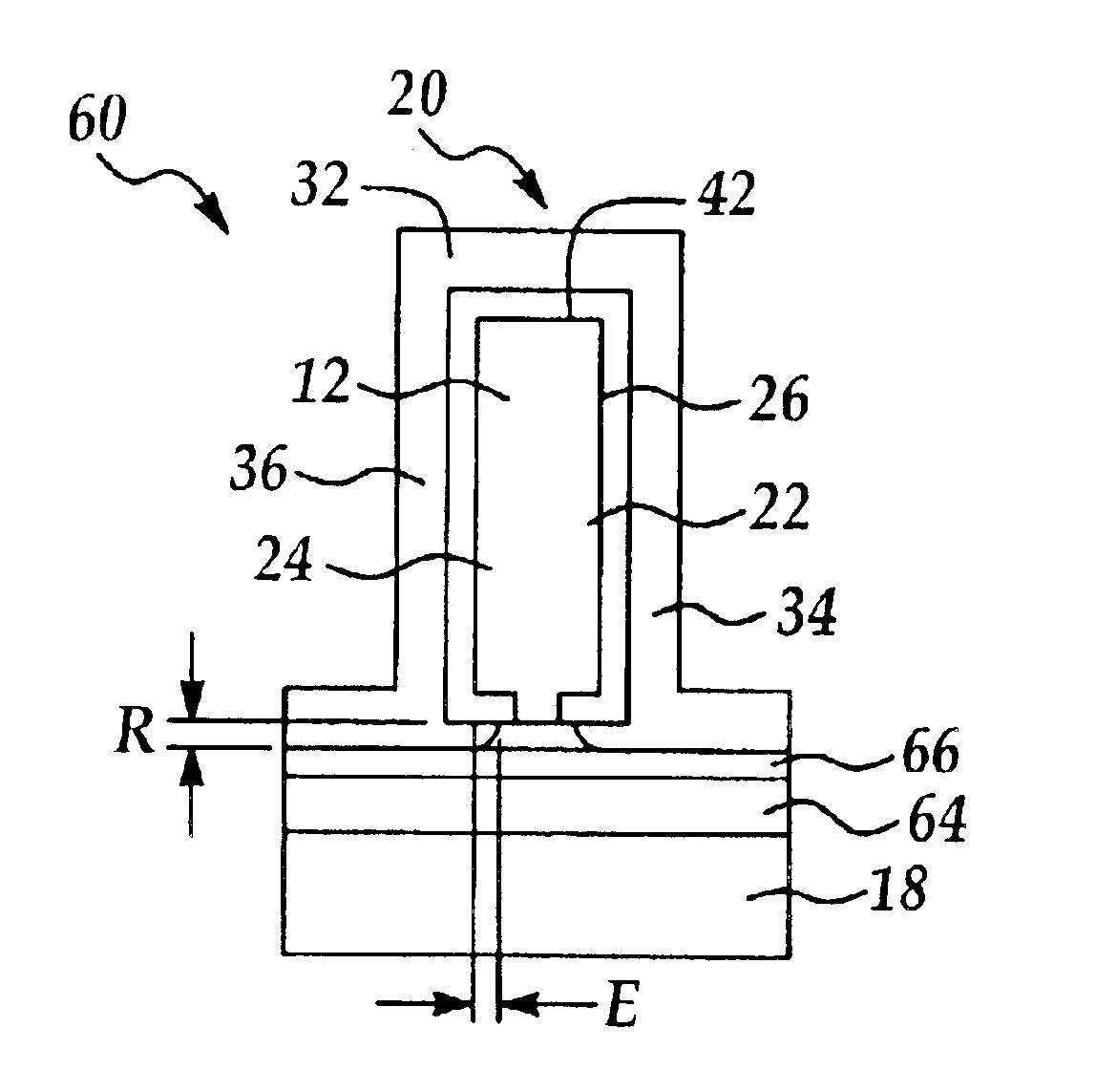
The present invention provides an improved process wherein an etch stop layer is used to control the amount of recess R. It achieves accurate control of the recess and an improved process window with little variability. The improved process, i.e., the preferred embodiment of the present invention, is schematically described in FIG. 5A-5E. FIGS. 5A-5E show the device cross-sections at the various process steps, as observed along line A-A′ in the plane view for the completed device in FIG. 6. The starting substrate is a silicon-on-insulator substrate, as shown in FIG. 5A. The starting substrate comprises of a silicon film 58 overlying an insulator stack 62. The insulator stack 62 comprises of a first insulator layer 68 overlying an etch-stop 66 layer which overlies a second insulator layer 64. The first insulator layer 64 can be made of any first dielectric material such as silicon oxide. The first insulator layer 68 has a thickness of between 20 angstroms and 1000 angstroms. The seco...
PUM
 Abstract
Description
Claims
Application Information