Fabrication method of nitride-based semiconductors and nitride-based semiconductor fabricated thereby

a technology of nitride-based semiconductors and fabrication methods, which is applied in the direction of polycrystalline material growth, crystal growth process, chemistry apparatus and processes, etc., can solve the problems of excessive effort, crystal defects deterioration properties, and hardly grown high-quality nitride single crystals on substrates, etc., to reduce stress and resultant dislocation, increase quantum efficiency

Active Publication Date: 2005-01-18
SAMSUNG ELECTRONICS CO LTD
View PDF4 Cites 104 Cited by
  • Summary
  • Abstract
  • Description
  • Claims
  • Application Information

AI Technical Summary

Benefits of technology

It is therefore an object of the present invention to provide a fabrication method of nitride-based semiconductors capable of forming a nanoscale uneven structure on a sapphire subst

Problems solved by technology

However, because the substrate material such as sapphire is not identical with GaN in lattice constant and thermal expansion coefficient, high quality nitride single crystal is hardly grown on the substrate.
However, a nitride layer grown in this solution contains crystal defects up to about 109 to 1010 cm−2.
Crystal defects deteriorate properties of resultant nitride-based semiconductors.
However,

Method used


Image

  • Fabrication method of nitride-based semiconductors and nitride-based semiconductor fabricated thereby
  • Fabrication method of nitride-based semiconductors and nitride-based semiconductor fabricated thereby
  • Fabrication method of nitride-based semiconductors and nitride-based semiconductor fabricated thereby

Examples


Embodiment Construction

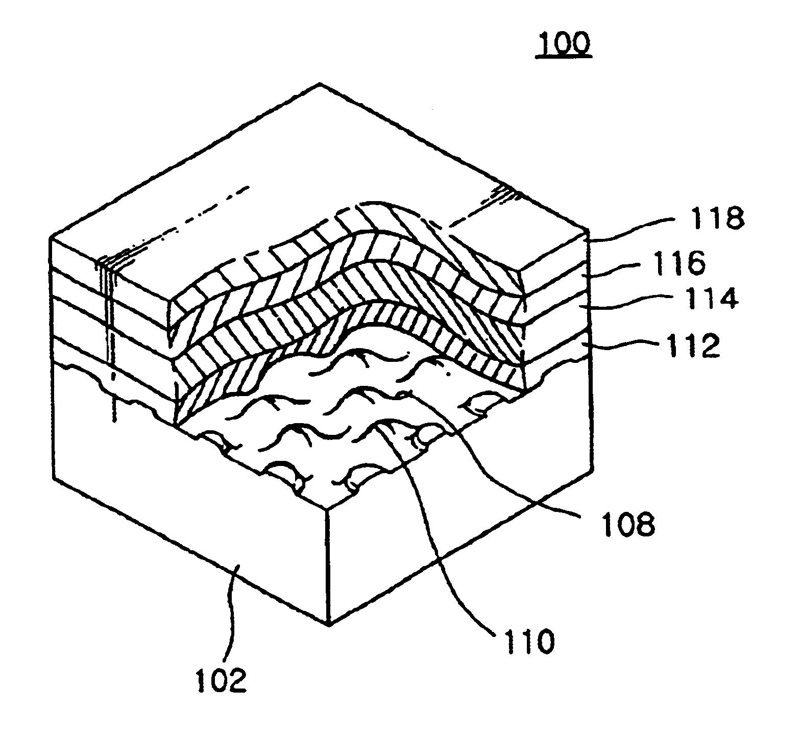
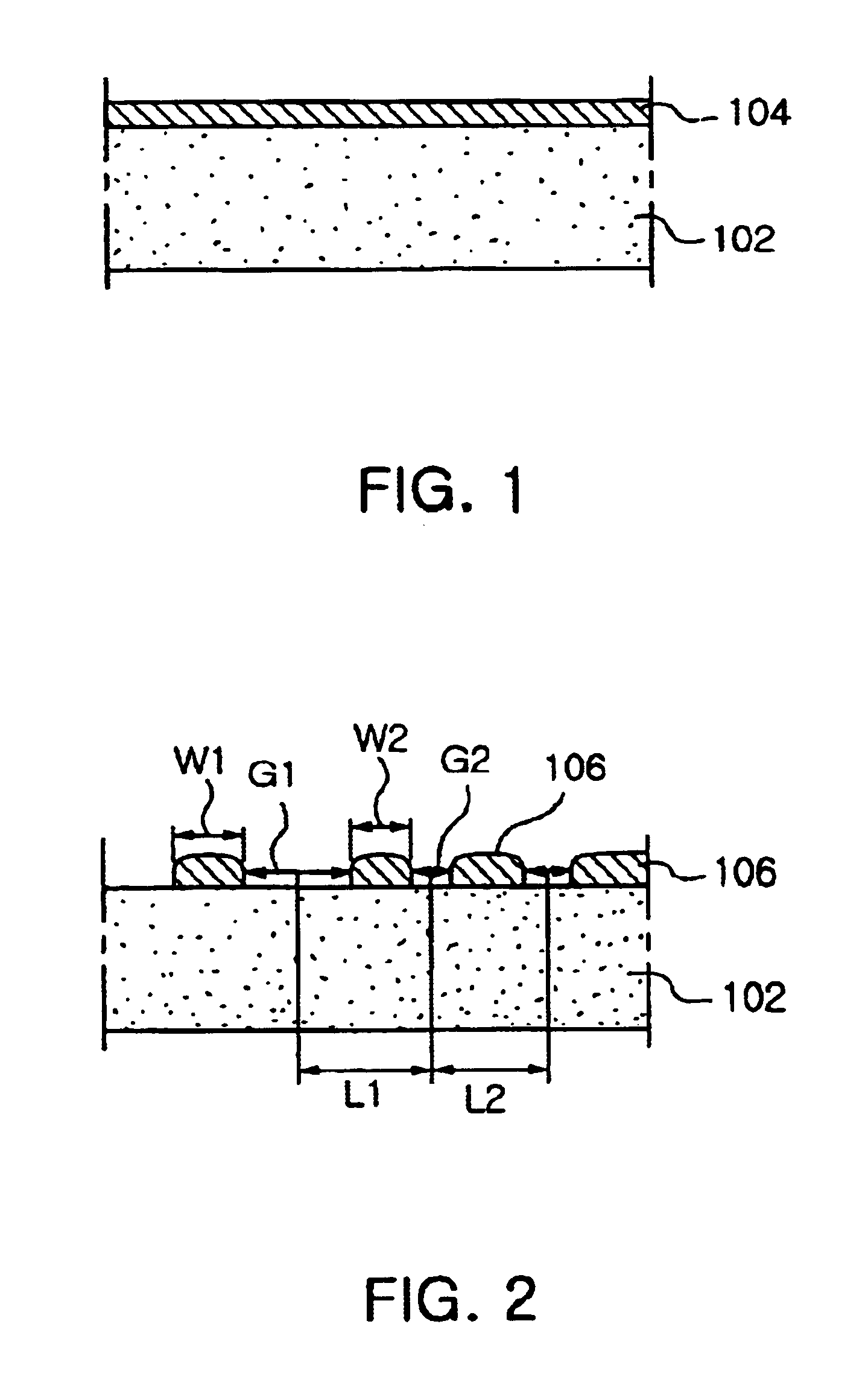
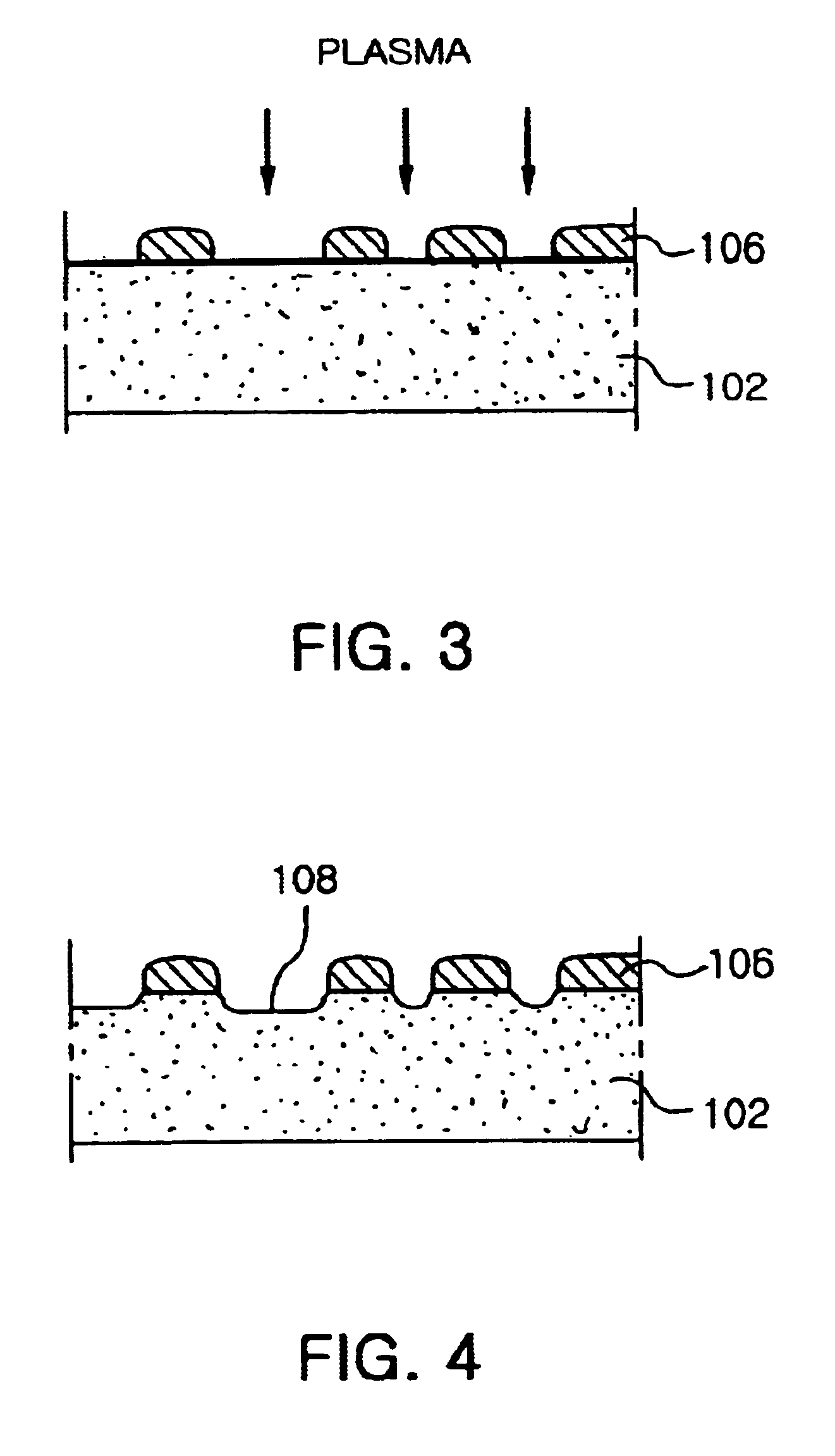
The present invention proposes to form a nanoscale uneven structure on a sapphire substrate so that the nanoscale roughened sapphire substrate can be utilized in fabrication of nitride-based semiconductors. The nanoscale uneven structure on the sapphire substrate has an effect on GaN nucleation in a GaN-growing process to decrease crystal defects of GaN compound formed on the sapphire substrate. In detail, this restrains GaN growth around pores of the sapphire substrate but accelerates GaN nucleation around projections of the sapphire substrate so as to decrease any defects or faults in the interference between the sapphire substrate and GaN nuclei.

Referring to total reflection conditions, reflection angle is determined by the index of reflection between a sapphire substrate and air or GaN compound and air. If reflection angle is smaller than critical angle, light cannot escape out of a device. The invention overcomes this problem by means of a nanoscale uneven structure formed on t...


PUM


Abstract

The present invention relates to a fabrication method of nitride-based semiconductors and a nitride-based semiconductor fabricated thereby. In the fabrication method of the invention, a self-organizing metal layer is formed on a sapphire substrate. The sapphire substrate having the self-organizing metal layer is heated so that self-organizing metal coalesces into nanoscale clusters to irregularly expose an upper surface of the sapphire substrate. Exposed portions of the sapphire substrate is plasma etched using the self-organized metal clusters as a mask to form a nanoscale uneven structure on the sapphire substrate. A resultant structure is wet etched to remove the self-organized metal clusters. The nanoscale uneven structure formed on the sapphire substrate decreases the stress and resultant dislocation between the sapphire substrate and a nitride-based semiconductor layer as well as increases the quantum efficiency between the same.

Description

BACKGROUND OF THE INVENTION1. Field of the InventionThe present invention relates to a nitride-based semiconductor. In particular, the present invention relates to a fabrication method of nitride-based semiconductors capable of forming a nanoscale uneven structure on a sapphire substrate to decrease the stress and resultant dislocation between the sapphire substrate and a nitride-based semiconductor layer while increasing the quantum efficiency between the same. The invention also relates to a nitride-based semiconductor fabricated according to the above fabrication method of nitride-based semiconductors.2. Description of the Related ArtA Light Emitting Diode (LED) basically consists of a junction of p- and n-doped semiconductor layers formed on a sapphire substrate as a kind of optoelectric device. When applied with electric current, the electron-hole combination in the LED converts energy corresponding to its band gap into light.The semiconductor layers of the LED a re obtained by...

Claims


Application Information

Patent Timeline
IPC IPC(8): H01L33/00C30B29/60H01L21/3065H01L21/20H01L21/205H01L33/22H01L33/32
CPCC30B29/605H01L21/0237H01L21/0242H01L33/007H01L21/02458H01L21/0254H01L21/02658H01L21/0243H01L33/22
Inventor LEE, KYU HANKIM, SUN WOONKIM, JE WON
Owner SAMSUNG ELECTRONICS CO LTD
Why Eureka
Try Eureka