Semiconductor pressure sensor device protected with perfluoropolyether gel

a technology of perfluoropolyether and pressure sensor, which is applied in the direction of fluid pressure measurement, instrumentation, and device details of the semiconductor/solid-state device, can solve the problems of gel material cracking, insulating/protecting function, and sensor function itself being lost, so as to improve the adhesive strength of the rubber material to any mating material, and reduce the tg of the rubber material

Inactive Publication Date: 2005-01-18
SHIN ETSU CHEM IND CO LTD
View PDF8 Cites 19 Cited by
  • Summary
  • Abstract
  • Description
  • Claims
  • Application Information

AI Technical Summary

Benefits of technology

Like the fluorochemical gel material, the fluorochemical rubber material used herein can be a cured product of a curable composition comprising a polymer of hexafluoropropylene oxide as a base polymer. The rubber material has a Tg of −45° C. or lower (embrittlement temperature −20° C. or lower) and a degree of saturation swelling in gasoline at 23° C. of 7% by weight or less. Like the gel material, the Tg of the rubber material can be lowered by selecting the type and amount of the non-functional perfluoropolyether (E). The fluorochemical rubber material may further contain a carboxylic acid anhydride, and in this embodiment, the rubber material is more effective for restraining bubble generation from voids between the housing and the leads because the adhesive strength of the rubber material to any mating material is enhanced.

Problems solved by technology

Bubbles generated therefrom will grow or travel with a change of temperature or pressure and cause cracking to the gel material or breakage to the bonding wires.
Then not only the insulating / protecting function, but the sensor function itself is lost.
On the other hand, even in the case of the semiconductor pressure sensor encapsulated with a fluorochemical gel material having a degree of saturation swelling in gasoline at 20° C. of up to 7 wt % and a Tg of up to −30° C., if the gel material has a high penetration, the gel material, when subjected to pressure cycling in a low-temperature state below 0° C. over a long period of time, undergoes initial bubble formation and eventual liquefaction, resulting in a portion thereof flowing out of the cavity and interfering with the insulating / protecting function.

Method used


Image

  • Semiconductor pressure sensor device protected with perfluoropolyether gel
  • Semiconductor pressure sensor device protected with perfluoropolyether gel
  • Semiconductor pressure sensor device protected with perfluoropolyether gel

Examples


first embodiment

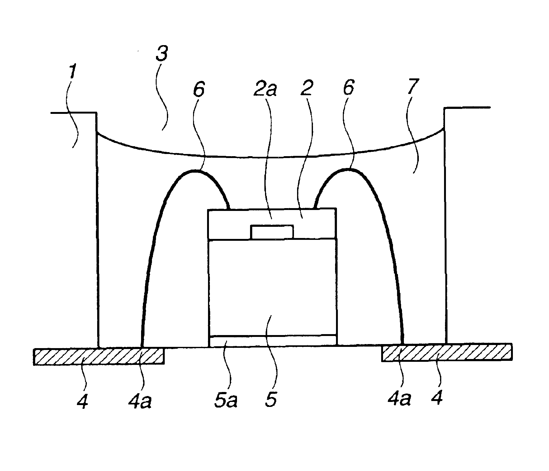
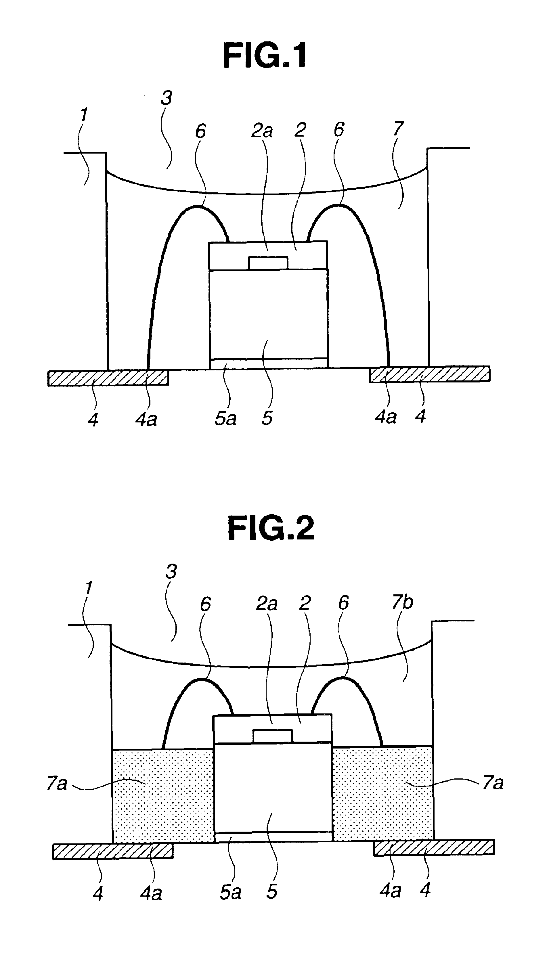
Referring to FIG. 1, there is illustrated in elevational cross-section a semiconductor pressure sensor device according to the first embodiment of the invention. A resinous housing 1 is made of a filled resin such as an epoxy resin, polyphenylene sulfide (PPS) or polybutylene terephthalate (PBT) and defines a cavity 3 where a semiconductor sensor chip 2 is to be mounted.

The resinous housing 1 has been molded over a plurality of insert pins 4 (also referred to as “leads,” herein) made of an electrically conductive material such as copper by an insert molding technique so that the insert pins 4 are embedded in the housing 1. Of the plurality of insert pins 4, four insert pins are located at the four corners of the cavity 3 at the bottom and exposed thereat within the cavity 3. The exposed portions of the insert pins 4 are plated with gold and serve as bonding pads 4a.

The semiconductor sensor chip 2 used herein is a sensor chip of well-known construction utilizing a piezoresistance ef...

second embodiment

While the first embodiment described above relies on the protective material consisting of a single fluorochemical gel material, the second embodiment differs therefrom in that the protective material consists of two species of material having different modulus of elasticity due to different crosslinking density.

Referring to FIG. 2, there is illustrated in elevational cross-section a semiconductor pressure sensor device according to the second embodiment of the invention. Since the second embodiment contains the same elements in substantially the same configuration as in the first embodiment except for the above difference, like parts in FIGS. 1 and 2 are designated by the same numerals for the sake of brevity of description.

In the device of the second embodiment, the protective material 7 filled in the cavity 3 for covering the sensor chip 2 and bonding wires 6 has a two-layer structure consisting of a first protective material 7a on the lower layer side (cavity bottom side) and a ...

preparation example 1

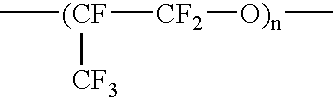
In 100 parts of a polymer having formula A-1 (viscosity 2,100 cSt) and 33 parts of a polymer having formula E-1, 1.5 parts of Aerosil R-976 (Nippon Aerosil Co., Ltd.) was compounded. This was combined with 0.3 part of a 50% toluene solution of ethynyl cyclohexanol, 0.2 part of a toluene solution containing a vinylsiloxane complex of chloroplatinic acid (platinum metal concentration 0.5 wt %), 6.2 parts of a compound having formula C-1, 1.5 parts of a compound having formula C-2, and 1.5 parts of a compound having formula G-1. These components were uniformly mixed to form a rubber composition 1.

The composition was press molded at 150° C. for 10 minutes and post-cured at 150° C. for 50 minutes, yielding a rubber material 1. The physical properties (hardness, tensile strength and elongation) of the cured part were measured according to JIS K6249. The degree of saturation swelling in gasoline (using unleaded gasoline) was measured according to JIS K6258 under immersion conditions: 23° C...


PUM

PropertyMeasurementUnit
glass transition temperatureaaaaaaaaaa
temperatureaaaaaaaaaa

Abstract

In a semiconductor pressure sensor device comprising a housing (1) having a cavity (3), a semiconductor sensor chip (2) mounted within the cavity, leads (4) for conveying pressure detection signals, and bonding wires (6) electrically connecting the sensor chip and the leads, a sensitive portion (2a) of sensor chip (2), leads (4) and bonding wires (6) are covered with an electrically insulating fluorochemical gel material which has a penetration of 30-60 according to JIS K2220, a Tg of up to −45° C., and a degree of saturation swelling in gasoline at 23° C. of up to 7% by weight. The sensor device is improved in operation reliability and durability life.

Description

This invention relates to a semiconductor pressure sensor device in which a semiconductor sensor chip for detecting a pressure is mounted within a resinous housing, and the sensor chip and electrical connections are covered and protected with a fluorochemical material and which possesses improved operation reliability and durability life in an environment of gasoline vapor or corrosive gases.BACKGROUND OF THE INVENTIONFrom the past, semiconductor pressure sensors are used for measuring the pressure of intake and exhaust gases in automotive engines, the pressure of exhaust gases in motorcycle engines, and the like. For instance, pressure sensors for measuring the engine intake pressure in automobiles generally use semiconductor pressure sensor chips utilizing piezoresistance effect as the pressure detecting device. Semiconductor pressure sensor chips of this type are designed to detect as an electrical signal a change of resistance in response to any deformation of a diaphragm made o...

Claims


Application Information

Patent Timeline
Patent Type & Authority Patents(United States)
IPC IPC(8): G01L9/00C08K3/36C08K5/541C08L71/02C08L83/05H01L29/84
CPCG01L19/147H01L2224/48091H01L2224/73265H01L2224/8592H01L2924/00014H01L29/84
Inventor SHIONO, MIKIOFUKUDA, KENICHI
Owner SHIN ETSU CHEM IND CO LTD
Why Eureka
Try Eureka