Multilayer printed wiring board

a multi-layer printed, wiring board technology, applied in weaving, applications, other domestic objects, etc., can solve the problems of increasing the likelihood of glass cloth drill bit breakage, difficult to reduce the thickness of multi-layer printed wiring boards, and difficulty in increasing the density of each wiring pattern, so as to increase the contact area, increase the elastic modulus, and enhance the adhesion of resin

Inactive Publication Date: 2005-01-25
FUJITSU LTD
View PDF17 Cites 14 Cited by
  • Summary
  • Abstract
  • Description
  • Claims
  • Application Information

AI Technical Summary

Benefits of technology

In a preferred embodiment, the core member includes a plurality of glass clothes arranged at a pitch of 50-100 μm thicknesswise of the core member. More preferably, the number of glass clothes provided is in the range of 2-20. Herein, the pitch means the shortest distance between the thicknesswise center of one glass cloth and that of an adjacent glass cloth. In another preferred embodiment, the glass cloth constitutes 45-70 volume percent of the core member. Due to such an arrangement and volume percentage of the glass cloth, the core member can maintain a high elastic modulus.
Preferably, each of the glass filaments of the glass cloth has a diameter of 3-7 μm. More preferably, the glass filament has a diameter of 3-5 μm. By using such thin filaments, it is possible to increase the contact area between the resin and the glass cloth in the core member for enhancing adhesion of the resin and the glass cloth. Moreover, when the glass filament has a diameter in the range of 5-7 μm, the formation of vias in the core member is facilitated.

Problems solved by technology

With such a method, however, it is difficult to reduce the thickness of the multilayer printed wiring board because each of the copper-clad laminates and prepregs is relatively thick due to its inclusion of a glass cloth.
Moreover, it is also difficult to increase the density of each wiring pattern because each of the holes for the vias generally has a large diameter of about 0.3 mm or more.
If the diameter of a hole is decreased for enhancing the wiring density, the likelihood of breakage of the drill due to the glass cloth increases.
Moreover, when the number of copper-clad laminates is increased, a drill of a larger diameter capable of perforating such a large number of layers need be used, which causes an increase in diameter of the holes and bars the provision of a wiring pattern having a high density.
However, as compared with a wiring board formed by the laminating and pressing method, a buildup-type multilayer printed wiring board formed by the conventional buildup method warps largely as a result of reflow soldering performed in the manufacturing process or in the process of mounting electronic components thereon.
If a wiring board largely warps, undesirably non-contacting bumps may be provided, causing connection failure between electrode pads which are otherwise duly connected.
The problem of warping of the wiring board becomes more serious when the volume ratio of the buildup layers increases as a result of laminating a large number of the buildup layers.
However, treatment of the multilayer printed wiring board at such a high temperature causes the wiring board to warp largely.
With such a method, however, the thickness of the multilayer printed wiring board cannot be reduced due to the thick core member.
However, the forming of insulating layers i.e., build up layers from a prepreg increases the thickness of the wiring board.
Therefore, also in this case, it is not possible to respond to the demand for thickness reduction of the wiring board.
However, none of these techniques can realize high density of the wiring pattern and sufficient decrease in the warping amount of the wiring board.

Method used


Image

  • Multilayer printed wiring board
  • Multilayer printed wiring board
  • Multilayer printed wiring board

Examples


embodiment 1

[Measurement of Elastic Modulus]

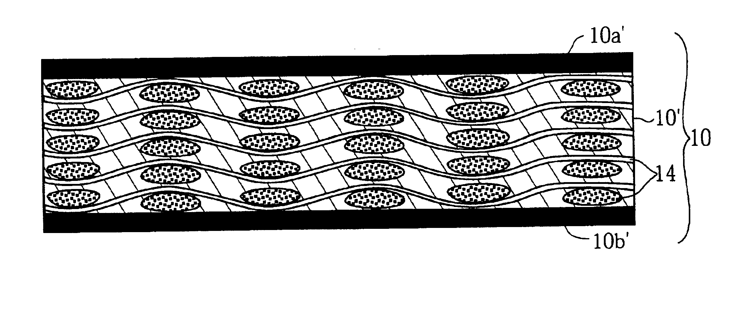
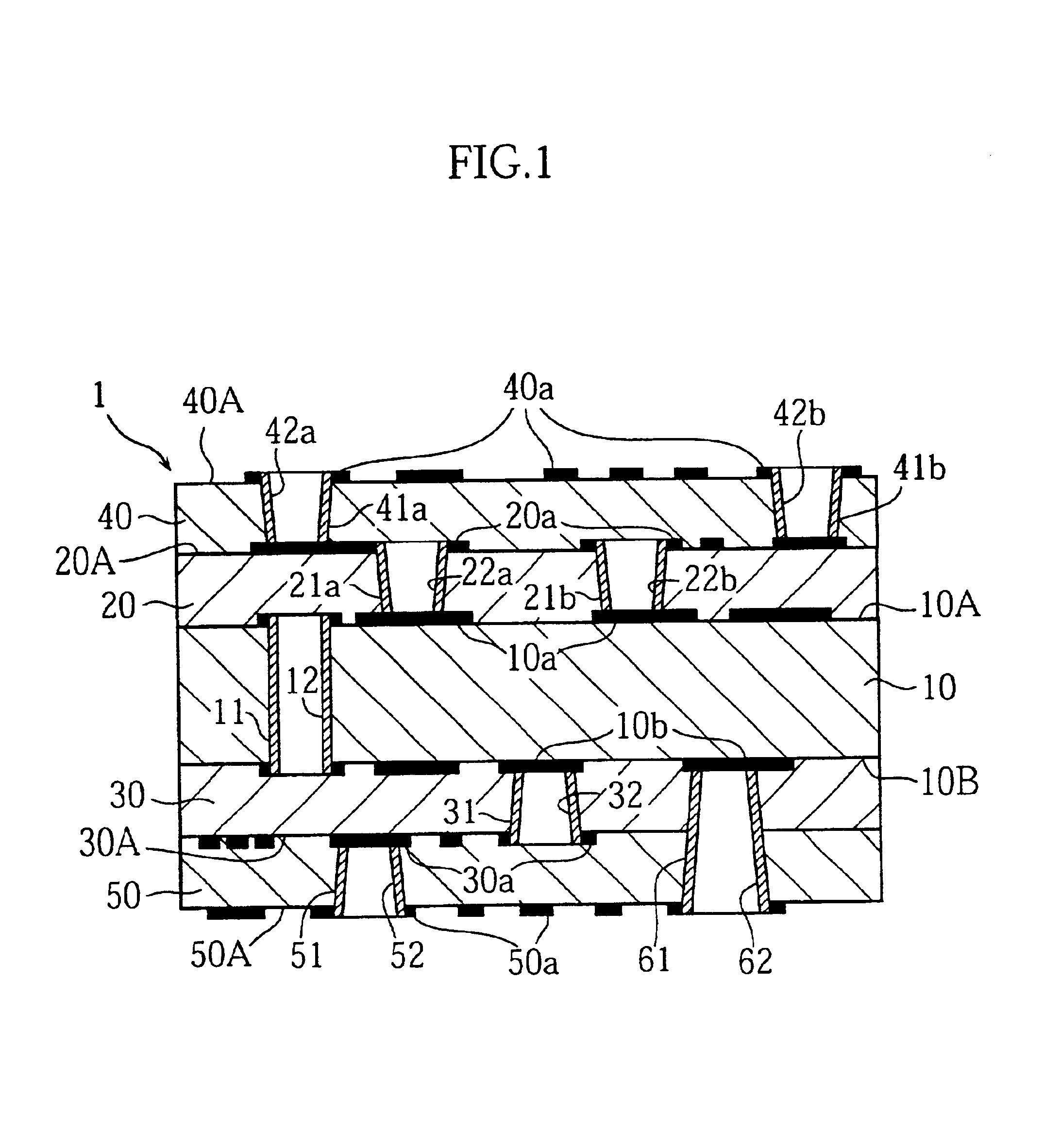
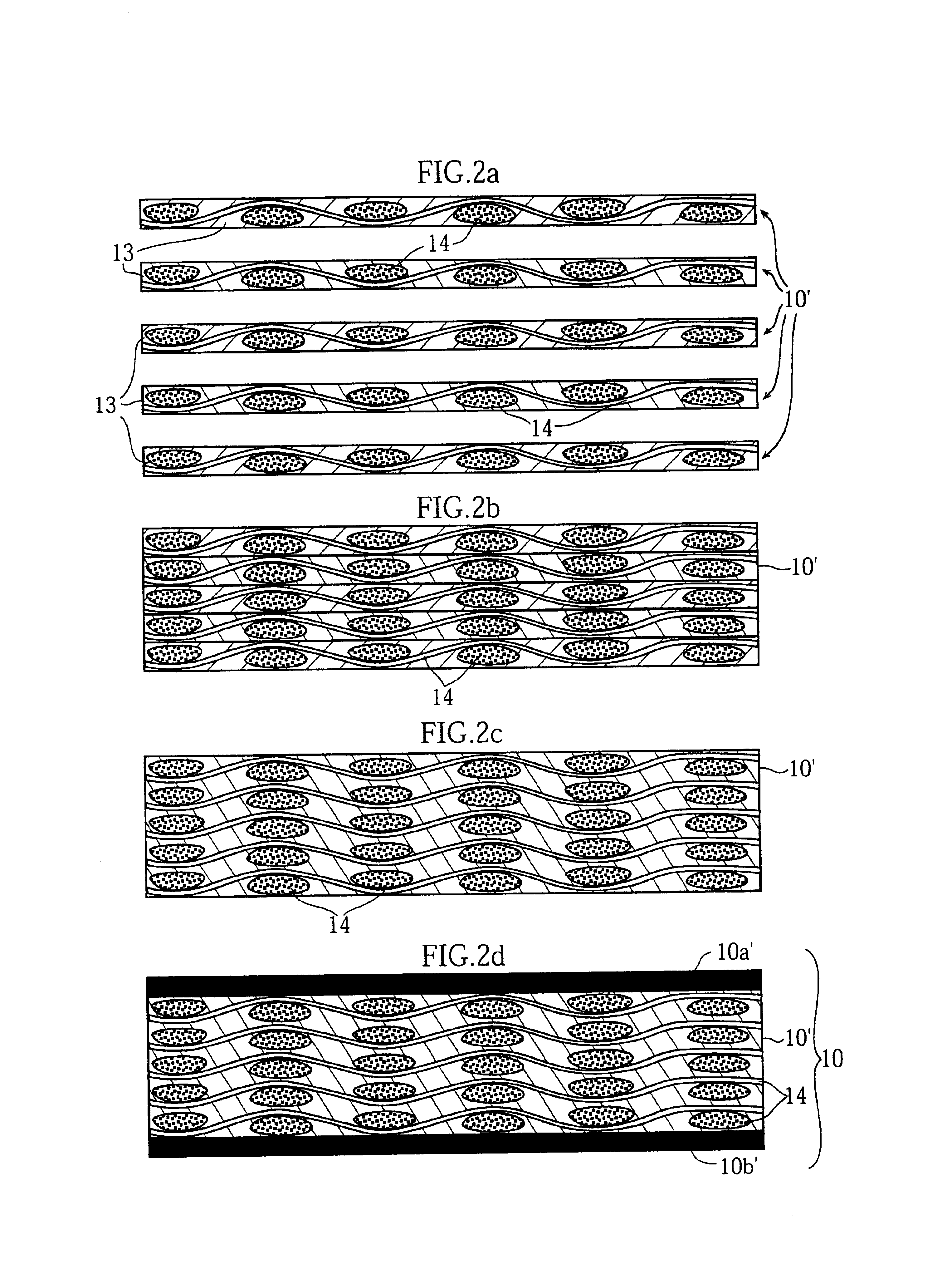
In Embodiment 1, use was made of a core member (Tradename: H-32, Supplier: Showa Denko K. K) which had a thickness of 0.4 mm and a workpiece size of 340×510 mm. The core member contained 50 volume % of glass cloth. The core member was a laminate of prepregs each prepared by impregnating a glass cloth (E-glass) with an epoxy resin, and attaching copper foils to the opposite surfaces of the prepreg laminate. The glass cloth comprised filaments each having a diameter of 5 μm. The epoxy resin contained, as dispersed therein, powder of aluminum hydroxide having an average particle size of 3.8 μm. Each of the copper foils had a thickness of 18 μm.

Further, epoxy resin sheets (Tradename: ABF-SH, Supplier: Ajinomoto Co., Inc.) were used as insulating films for forming buildup layers. Each of the resin sheets had a thickness of 50 μm.

The bending elastic modulus of the core member was measured by the three-point bending method using an elastic modulus measuring ...

embodiment 2

[Measurement of Elastic Modulus]

In Embodiment 2, use was made of a core member which had a thickness of 0.4 mm and a workpiece size of 340×510 mm. The core member contained 45 volume % of glass cloth. The core member was a laminate of prepregs each prepared by impregnating a glass cloth with an epoxy resin, and attaching copper foils to the opposite surfaces of the prepreg laminate. The glass cloth comprised filaments each having a diameter of 7 μm. The epoxy resin contained, as dispersed therein, powder of magnesium hydroxide having an average particle size of 3 μm and powder of silica having an average particle size of 4 μm. Each of the copper foils had a thickness of 18 μm.

Further, polyimide resin sheets were used as insulating films for forming buildup layers. Each of the resin sheets had a thickness of 30 μm.

As a result of the elastic modulus measurement performed in the same way as in Embodiment 1, the core member was found to have a bending elastic modulus of 14 GPa at 240° C...

embodiments 4-12

A plurality of multilayer printed wiring boards which included 2-10 buildup layers on each surface of the respective core member were prepared in the same manner as in Embodiment 3. The respective warping amounts (maximum gaps) of these wiring boards were measured before and after the wiring boards were subjected to the reflow process ten times. The measurement results of the wiring boards including 2˜10 buildup layers are given in Table 1 as Embodiments 4˜12, respectively.


PUM

PropertyMeasurementUnit
elastic modulusaaaaaaaaaa
diameteraaaaaaaaaa

Abstract

A multilayer printed wiring board includes a core member having a plurality of glass clothes impregnated with a resin. Each of the glass clothes is woven with glass yarns each of which includes a bundle of glass filaments. One or more buildup layers are laminated on one or each surface of the core member. The core member has an elastic modulus which is no less than 100 times that of the buildup layer at 240° C.

Description

BACKGROUND OF THE INVENTION1. Field of the InventionThe present invention relates to a multilayer printed wiring board for use in electric or electronic components. More particularly, the present invention relates to a multilayer printed wiring board comprising a core member and buildup layers laminated on the core member.2. Description of the Related ArtDue to the need for increasing the wiring density of an electric / electronic circuit for use in electric / electronic devices, a multilayer printed wiring board including a plurality of conductive layers for mounting electronic components is widely used. Such multilayer printed wiring boards are generally divided into two groups in accordance with the manufacturing method.One method for forming a multilayer printed wiring board comprises laminating a predetermined number of copper-clad laminates while interposing a prepreg between the two adjacent copper-clad laminates and then pressing the laminated layers under a certain pressure in ...

Claims


Application Information

Patent Timeline
Patent Type & Authority Patents(United States)
IPC IPC(8): B32B17/04B32B15/04B32B27/38D03D15/08H05K3/46H05K1/03D03D15/56
CPCB32B15/04B32B17/04B32B27/38B32B37/0015H05K1/0366H05K3/4602D03D15/08B32B2457/08Y10T428/24917H05K2201/0209H05K2201/029H05K2201/09536Y10T442/2041Y10T442/3008Y10T442/2418Y10T442/2049Y10T442/2475Y10T442/2926Y10T442/2992Y10T442/2951Y10T442/209Y10T442/2008D03D15/56
Inventor TANI, MOTOAKIHAYASHI, NOBUYUKIMACHIDA, HIROYUKIISHITSUKA, TAKESHIYAMAGISHI, YASUO
Owner FUJITSU LTD
Why Eureka
Try Eureka