
III-V compound semiconductor device with an AlxByInzGa1-x-y-zN1-a-bPaAsb non-continuous quantum dot layer

a semiconductor and compound layer technology, applied in the direction of nano-informatics, crystal growth process, polycrystalline material growth, etc., can solve the problems of high electric field breakdown, high thermal conductivity, direct band gap structure, etc., and achieve high recombination efficiency

Inactive Publication Date: 2005-02-01
KYMA TECH
View PDF58 Cites 33 Cited by
  • Summary
  • Abstract
  • Description
  • Claims
  • Application Information

AI Technical Summary

Benefits of technology

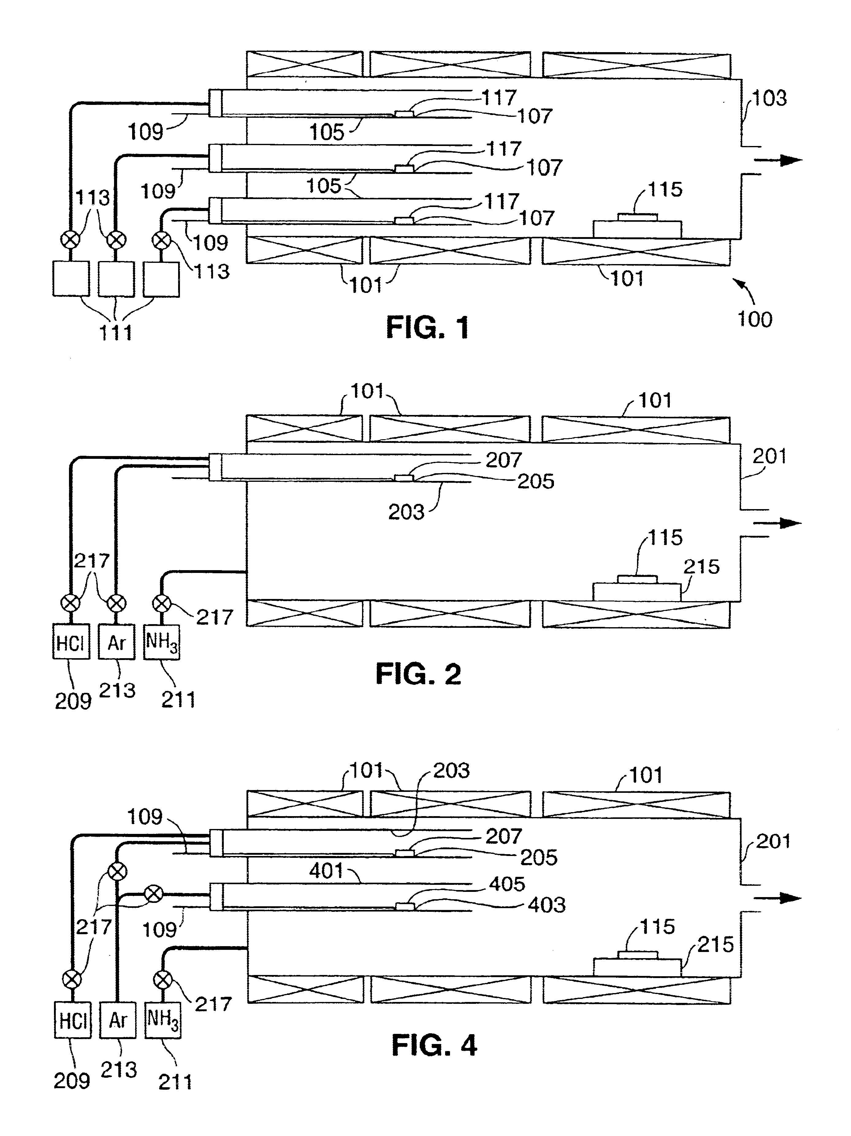
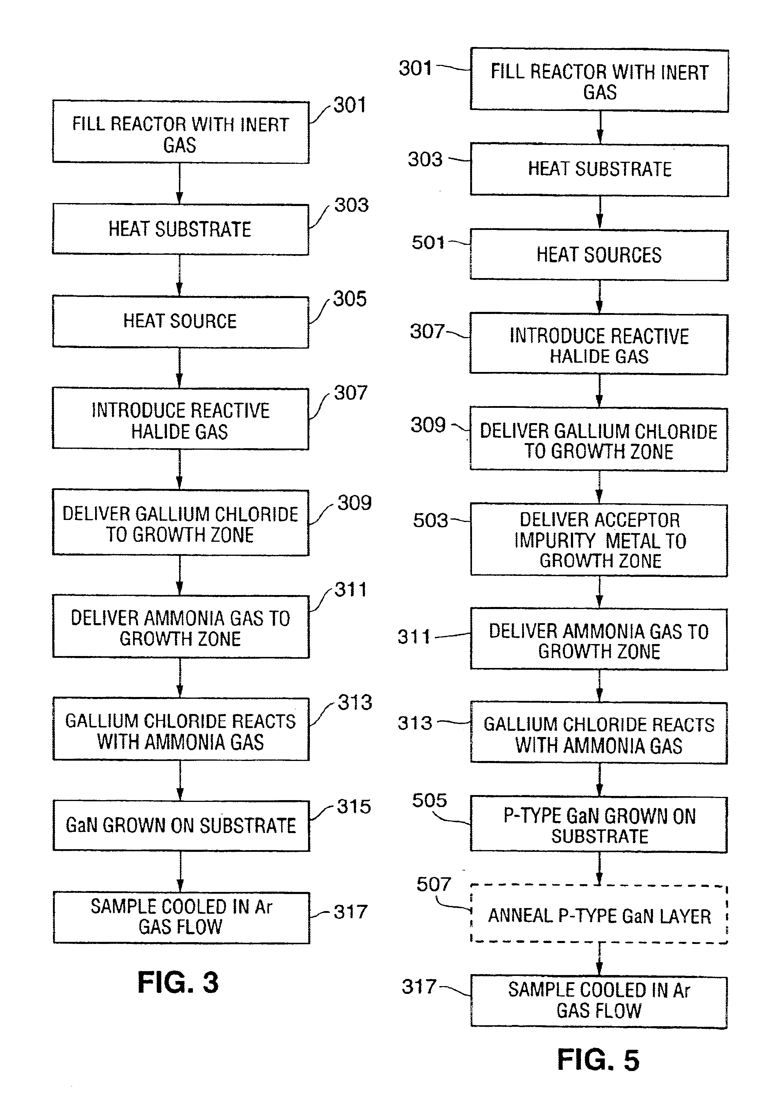
"The present invention provides a method for fabricating p-type III-V compounds using the HVPE technique. This allows for the growth of a variety of different devices using the invention. The method involves heating a furnace to a suitable temperature and exposing a Group III source to a halide reactive gas to form halide metal compounds. These compounds are then transported to the growth zone as is a reactive gas containing the desired Group V element. The resulting material growth is achieved through the reaction between the reactive gas and the halide metal compounds. The method can be used to fabricate p-n homojunction devices, p-n heterojunction devices, and double heterojunction devices. The invention also provides a simple p-n homojunction device and a simple p-n heterojunction device."

Problems solved by technology

In particular, these materials exhibit a direct band gap structure, high electric field breakdown, and high thermal conductivity.
Unfortunately, although the III-V compounds are attractive for semiconductor applications due to their physical and electronic properties, until recently the development of devices based on III-V compounds has been limited by the lack of material with suitable conductivity, specifically p-type material.
Although the MOCVD technique has proven adequate for a variety of commercial devices, it has a number of limitations that constrain the usefulness of this approach.
First, due to the complexity of the various sources (e.g., trimethylaluminum, trimethylgallium, and biscyclopentiadienylmagnesium), the process can be very expensive and one which requires relatively complex equipment.
Second, the MOCVD technique does not provide for a growth rate of greater than a few microns per hour, thus requiring long growth runs.
The slow growth rate is especially problematic for device structures that require thick layers such as high voltage rectifier diodes that often have a base region thickness of approximately 30 microns.
Conventional HVPE techniques have been unable, however, to grow such material.
As a result, the potential of the HVPE technique for fabricating p-n or p-i-n junction devices has not been realized.

Method used


Image

  • III-V compound semiconductor device with an AlxByInzGa1-x-y-zN1-a-bPaAsb non-continuous quantum dot layer
  • III-V compound semiconductor device with an AlxByInzGa1-x-y-zN1-a-bPaAsb non-continuous quantum dot layer
  • III-V compound semiconductor device with an AlxByInzGa1-x-y-zN1-a-bPaAsb non-continuous quantum dot layer

Examples


Embodiment Construction

"d_n">[0034]FIG. 15 illustrates a structure comprised of a narrow band gap material interposed between a pair of wide band gap materials;

[0035]FIG. 16 illustrates a low voltage drop device similar to the structure shown in FIG. 15;

[0036]FIG. 17 illustrates a device comprised of a p-n homojunction interposed between a pair of wide band gap material layers;

[0037]FIG. 18 illustrates an alternate device comprised of a p-n homojunction interposed between a pair of wide band gap material layers;

[0038]FIG. 19 illustrates yet another alternate device comprised of a p-n homojunction interposed between a pair of wide band gap material layers;

[0039]FIG. 20 illustrates yet another alternate device comprised of a p-n homojunction interposed between a pair of wide band gap material layers;

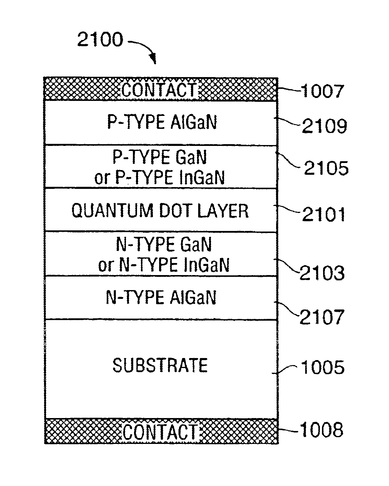
[0040]FIG. 21 illustrates a device comprised of a non-continuous quantum dot layer within a device's p-n junction;

[0041]FIG. 22 illustrates an alternate device comprised of a non-continuous quantum dot layer wit...


PUM


Abstract

A method for fabricating p-type, i-type, and n-type III-V compound materials using HVPE techniques is provided. If desired, these materials can be grown directly onto the surface of a substrate without the inclusion of a low temperature buffer layer. By growing multiple layers of differing conductivity, a variety of different device structures can be fabricated including simple p-n homojunction and heterojunction structures as well as more complex structures in which the p-n junction, either homojunction or heterojunction, is interposed between a pair of wide band gap material layers. The provided method can also be used to fabricate a device in which a non-continuous quantum dot layer is grown within the p-n junction. The quantum dot layer is comprised of a plurality of quantum dot regions, each of which is typically between approximately 20 and 30 Angstroms per axis. The quantum dot layer is preferably comprised of AlxByInzGa1-x-y-zN, InGaN1-a-bPaAsb, or AlxByInzGa1-x-y-zN1-a-bPaAsb.

Description

CROSS-REFERENCES TO RELATED APPLICATIONS[0002]This application is a continuation-in-part application of U.S. patent application Ser. No. 09 / 638,638, filed Aug. 14, 2000, now abandoned, which is a divisional of U.S. patent application Ser. No. 09 / 195,217 filed Nov. 18, 1998, now U.S. Pat. No. 6,218,269, which claims priority from U.S. patent application Ser. No. 60 / 066,940 filed Nov. 18, 1997, the disclosures of which are incorporated herein by reference for all purposes.FIELD OF THE INVENTION[0003]The present invention relates generally to semiconductor devices and, more particularly, to a method for fabricating p-n and p-i-n junction-based devices utilizing III-V compound layers as well as the structures that result from the application of the method.BACKGROUND OF THE INVENTION[0004]III-V compounds such as GaN, AlN, AlGaN, and InAlGaN have unique physical and electronic properties that make them ideal candidates for a variety of electronic and opto-electronic devices. In particular...

Claims


Application Information

Patent Timeline
Patent Type & Authority Patents(United States)
IPC IPC(8): C30B25/02H01L21/02H01L21/205H01L31/102H01L31/0264H01L31/0304H01L33/00H01L31/105
CPCB82Y10/00C30B25/02C30B29/40C30B29/403C30B29/406H01L21/0237H01L21/02378H01L21/02458H01L21/02505H01L21/0254H01L21/02543H01L21/02546H01L21/02579H01L21/0259H01L21/0262H01L31/0304H01L31/105H01L33/007B82Y30/00Y02E10/544
Inventor NIKOLAEV, AUDREY E.MELNIK, YURI V.VASSILEVSKI, KONSTANTIN V.DMITRIEV, VLADIMIR A.
Owner KYMA TECH
Learn More