Wear leveling techniques for flash EEPROM systems

a technology of flash eeprom and leveling techniques, applied in the field of mass digital data storage systems, to achieve the effect of extending the lifetime of the overall memory system, reducing the risk of wear and tear, and increasing the storage capacity

Inactive Publication Date: 2005-02-01
SANDISK TECH LLC
View PDF104 Cites 428 Cited by
  • Summary
  • Abstract
  • Description
  • Claims
  • Application Information

AI Technical Summary

Benefits of technology

If such an interchange, or wear leveling, is not carried out in the case where there is significantly uneven use among groups of EEPROM cells, one group will reach its end of lifetime while other groups have significant life left in them. When one group reaches an end of lifetime, the entire memory may have to be replaced unless extra groups of memory cells are included in the system for replacing those that reach their lifetime. However, the techniques of the present invention allow for extending overall memory system lifetime without having to provide such replacement groups of memory cells. The ability to interchange groups of cells to result in more even wear among the groups is particularly advantageous in computer system applications wherein flash EEPROM memory is used in the nature of a disk drive. This is because the memory is subjected to frequent erase and reprogramming cycles in some groups but not others, and since the large capacity of the memory would require a large number of spare groups in order to obtain a reasonable memory system lifetime without use of the group interchange technique of the present invention.

Problems solved by technology

If such an interchange, or wear leveling, is not carried out in the case where there is significantly uneven use among groups of EEPROM cells, one group will reach its end of lifetime while other groups have significant life left in them.

Method used


Image

  • Wear leveling techniques for flash EEPROM systems
  • Wear leveling techniques for flash EEPROM systems
  • Wear leveling techniques for flash EEPROM systems

Examples


Embodiment Construction

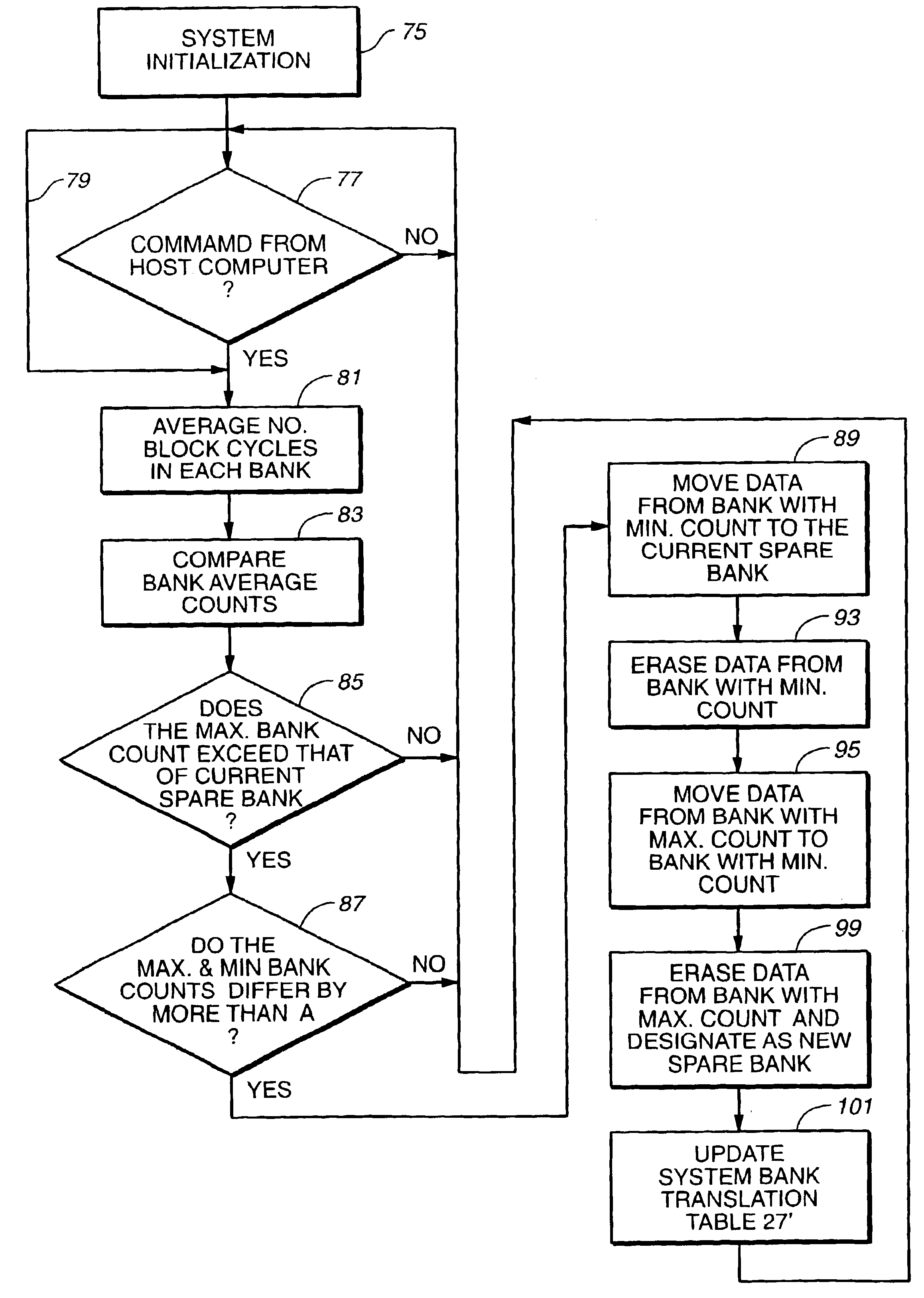
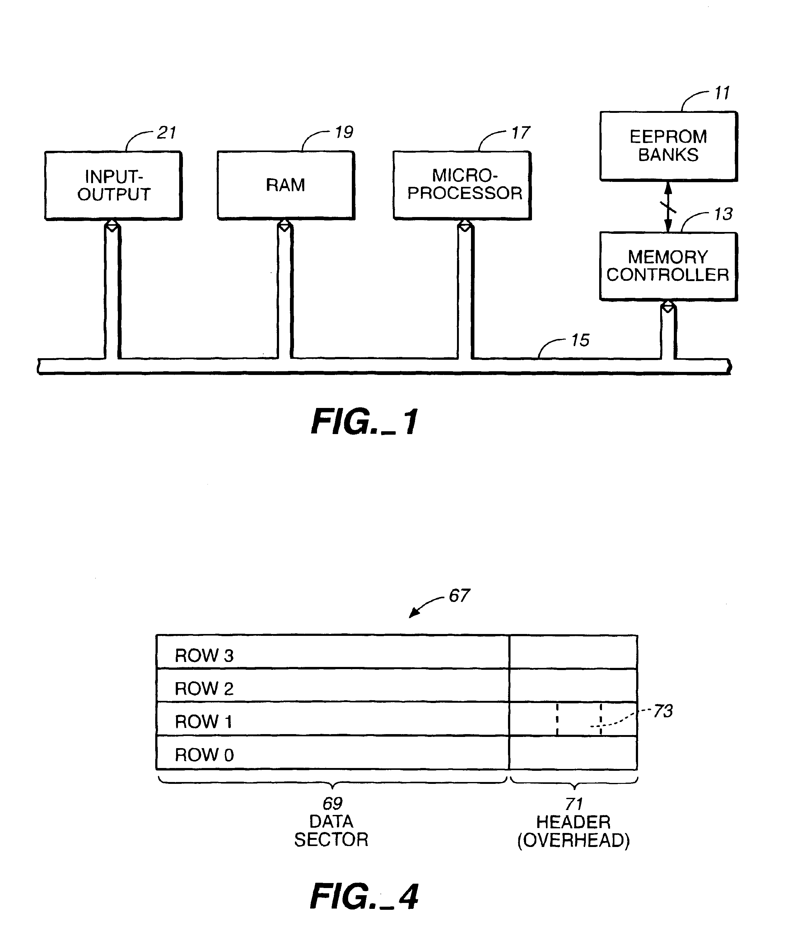
In order to set forth one environment in which the improved memory system of the present invention may be utilized, FIG. 1 shows a general computer system that includes flash EEPROM memory array 11 whose operation is controlled by a memory controller 13. The memory system 11 and 13 is connected to a computer system bus 15, to which also are connected a system controlling microprocessor 17, random access memory (“RAM”) 19, input / output circuits (“I / O”) 21, and various other components as appropriate for a specific computer system. In the improvements being described, the memory controller 13 manages operation of the EEPROM memory 11 in a way to maximize the lifetime of the memory system by avoiding uneven use of any one part of it.

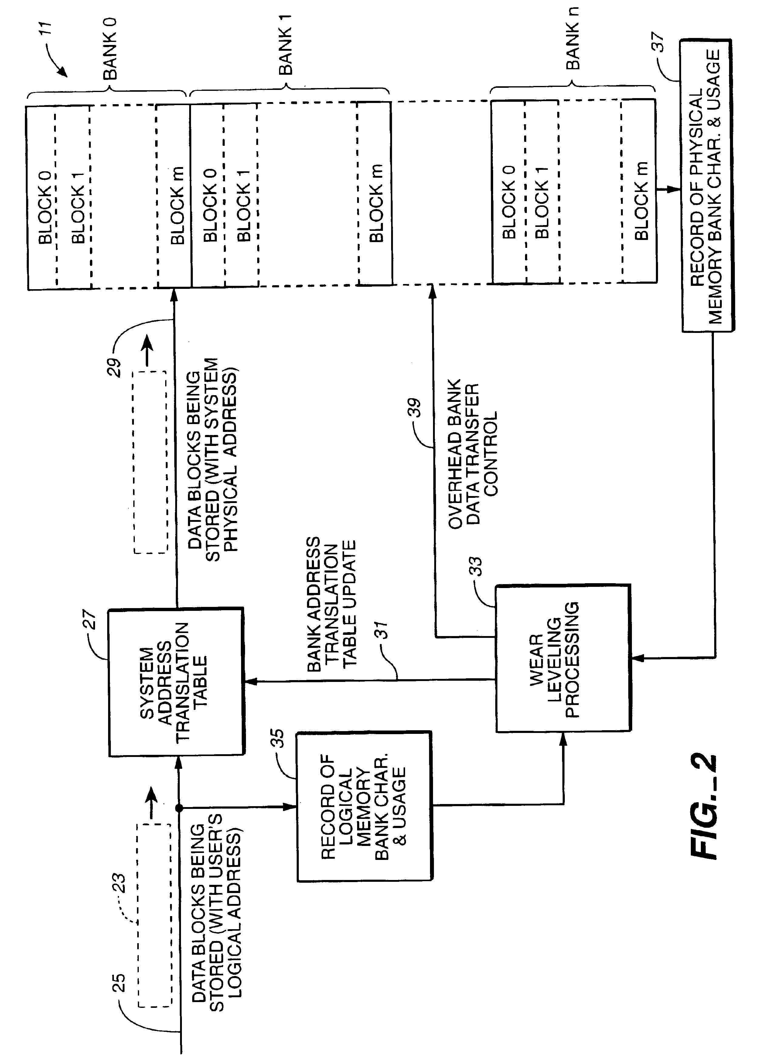
FIG. 2 is a diagram which conceptually and generally illustrates such a memory operation technique as well as showing various alternatives for specific implementations of the technique. The EEPROM memory 11 is organized into a large number of blocks of flas...


PUM


Abstract

A mass storage system made of flash electrically erasable and programmable read only memory (“EEPROM”) cells organized into blocks, the blocks in turn being grouped into memory banks, is managed to even out the numbers of erase and rewrite cycles experienced by the memory banks in order to extend the service lifetime of the memory system. Since this type of memory cell becomes unusable after a finite number of erase and rewrite cycles, although in the tens of thousands of cycles, uneven use of the memory banks is avoided so that the entire memory does not become inoperative because one of its banks has reached its end of life while others of the banks are little used. Relative use of the memory banks is monitored and, in response to detection of uneven use, have their physical addresses periodically swapped for each other in order to even out their use over the lifetime of the memory.

Description

BACKGROUND OF THE INVENTIONThis invention relates generally to mass digital data storage systems using flash electrically erasable and programmable read only memory (“EEPROM”) technology, and, more specifically, to techniques of controlling the use of such systems in order to improve their useful life.An advantage of using EEPROM technology is that a solid-state, non-volatile memory is provided, which can be repetitively reprogrammed. Each EEPROM cell includes an electrically floating gate positioned over a substrate channel between source and drain regions. A thin gate oxide layer separates the floating gate from the substrate. The threshold level of the cell is controlled by an amount of charge that is placed on the floating gate. If the charge level is above some threshold, the cell is read to have one state, and if below that threshold, is read to have another state.The desired floating gate charge level is programmed by applying an appropriate combination of voltages to the sou...

Claims


Application Information

Patent Timeline
Patent Type & Authority Patents(United States)
IPC IPC(8): G11C16/34G11C8/00G11C8/12G11C16/06
CPCG06F12/0246G11C16/349G11C16/3495G11C8/12G06F2212/1036G06F2212/7211
Inventor LOFGREN, KARL M. J.NORMAN, ROBERT D.THELIN, GREGORY B.GUPTA, ANIL
Owner SANDISK TECH LLC
Why Eureka
Try Eureka