Surface-type optical apparatus

a surface-type optical and optical apparatus technology, applied in the direction of material analysis using wave/particle radiation, instruments, nuclear engineering, etc., can solve the problems of unsuitable multiple arraying, unsuitable medium surface or the probe tip being likely to be damaged, and the coupling loss is likely to occur, so as to achieve rapid scanning, reduce the effect of coupling loss and low cos

Inactive Publication Date: 2005-02-08
CANON KK
View PDF18 Cites 27 Cited by
  • Summary
  • Abstract
  • Description
  • Claims
  • Application Information

AI Technical Summary

Benefits of technology

[0017]The minute opening is typically formed such that evanescent light is generated thereby. The minute opening is formed in a minute protrusion member, such as a tetrahedral metal member with an opening on its tip, provided at a light passing portion of the surface-type optical device, for example. When such a surface-type optical device is provided on a supporter, a highly-effective; light SNOM head, or the like, with little coupling loss can be achieved.
[0018]The surface-type optical device may be supported by the first substrate through an elastic supporter, and the first electrode wiring is formed on the first substrate and the elastic supporter. When the surface-type optical device is mounted on the elastic supporter, such as a thin-layer elastic supporter, a medium surface can be rapidly scanned without damages to the optical device and the medium surface. Further, arrayed SNOM heads or the like can be mounted on a common substrate through a single or plural elastic supporters.
[0019]The first substrate may be an Si substrate with an SiNx thin layer formed thereon, and the elastic supporter may be formed of a portion of the SiN, thin layer under which the Si substrate is removed. Thus, a compact elastic supporter, such as a cantilever-type thin-layer elastic supporter, can be readily fabricated.

Problems solved by technology

The structure illustrated in FIGS. 1 and 2, however, is undesirable, because light is guided through the optical fiber 603 and hence coupling loss is likely to occur.
Further, the SNOM head with the end-facet emitting laser 901, as illustrated in FIG. 4, is unsuitable for multiple arraying since its operational current and consumption electric power are large.
In such a structure, the medium surface or the probe tip is likely to be damaged unless the SNOM heads are supported by different elastic bodies to scan the medium surface while each probe tip precisely follows and traces the surface.
In such a structure, respective minute openings are present on a common plane, so that highly precise scanning of the medium surface is not possible.
Therefore, another optical system for optical detection is needed, so the apparatus becomes large in size.
Particularly where the arraying of the heads is to be designed, a preferable S / N of a detected signal is difficult to obtain due to the light interference and a relatively long distance between an observation point and a detecting system.
Therefore, the entire apparatus of the SNOM heads becomes large in size and heavy in weight, and hence a high-speed scanning is difficult to achieve.

Method used


Image

  • Surface-type optical apparatus
  • Surface-type optical apparatus
  • Surface-type optical apparatus

Examples


first embodiment

[0107](First Embodiment)

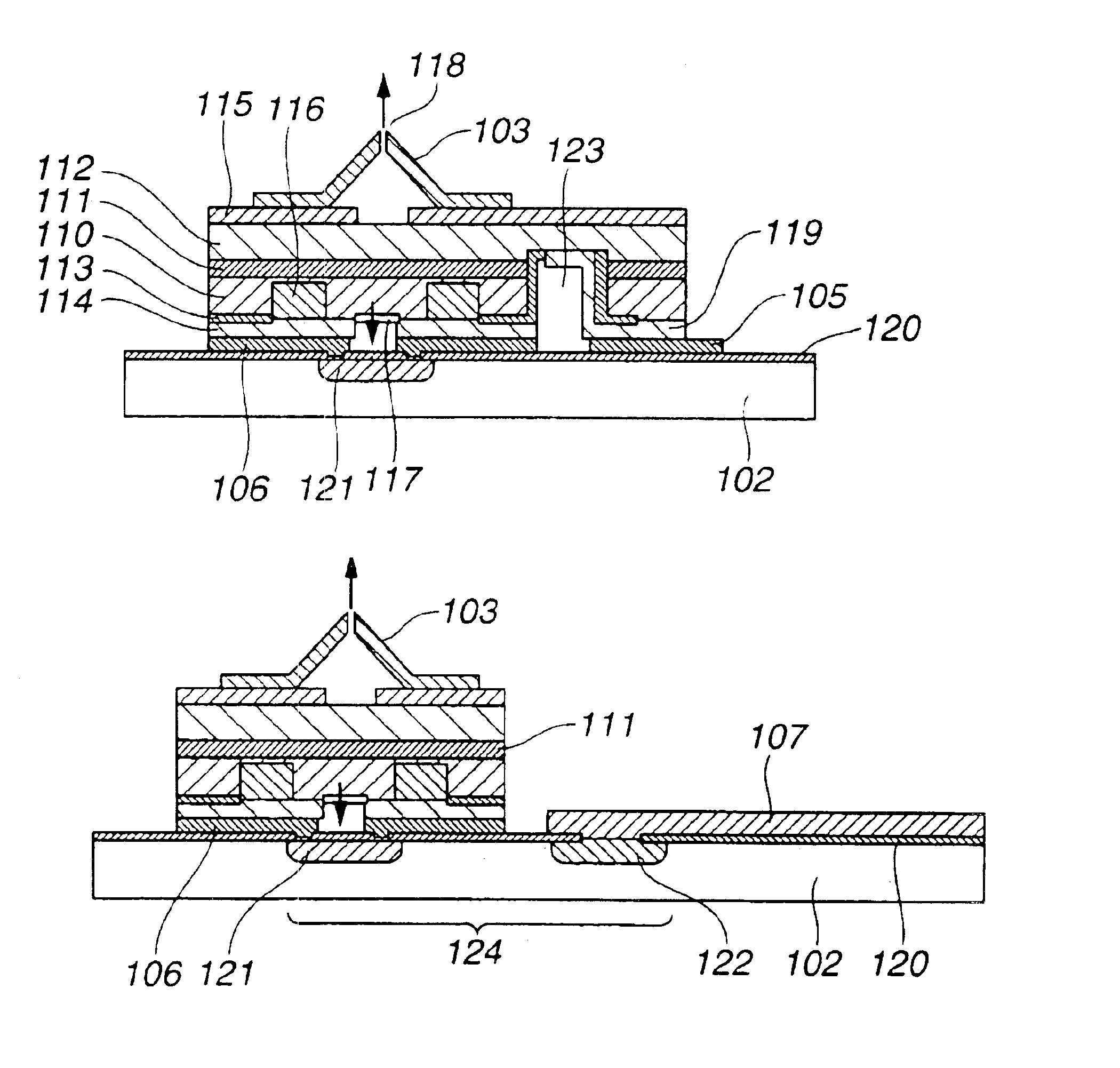
[0108]FIGS. 5A and 5B illustrate a first embodiment of a SNOM head of the present invention. The SNOM head includes a surface emitting laser, a protrusion member with a minute opening, which is formed on the surface of epitaxial layers of the laser, and a cantilever to a tip of which the laser with the protrusion member is mounted.

[0109]As illustrated in FIG. 5A of a perspective view and FIG. 5B of an A-A′ cross-sectional view of FIG. 5A, a surface emitting laser 4 used in this embodiment includes a one-wavelength cavity 12 consisting of an AlGaAs / GaAs multiple quantum well (MQW) active layer, an AlGaAs spacer layer, and n-type and p-type distributed Bragg reflector (DBR) mirrors 11 and 13 consisting of multiple (about twenty (20) to thirty (30) pairs) AlAs / AlGaAs layers of a ¼-wavelength thickness that sandwich the cavity 12. These layers are epitaxially grown on an n-GaAs substrate 10 by a metal organic vapor phase epitaxy (MOVPE), for example. An uppermost...

second embodiment

[0126](Second Embodiment)

[0127]A second embodiment of this invention is directed to a structure in which a surface emitting laser placed on the tip of a cantilever is further thinned to reduce its weight so that the size of the cantilever can be decreased and intervals between cantilevers reduced in a multi-lever structure.

[0128]FIG. 7 illustrates a cross section of the tip portion of the cantilever in the second embodiment. In FIG. 7, the reference numerals correspond to those in FIGS. 5A and 5B and denote portions having the same functions as those in FIGS. 5A and 5B. In the first embodiment, the GaAs substrate 10 with the functional portion of the laser thereon is bonded to the cantilever 8. In the second embodiment, however, an epitaxial layer side of the laser 4 is bonded to the cantilever 8, and the GaAs substrate 10 is fully removed by selective etching to leave only the epitaxial layers. The electrode 17 with the light-taking window and the protrusion member 3 with the minut...

third embodiment

[0138](Third Embodiment)

[0139]A third embodiment is directed to a structure in which both the p-side electrodes 16 and an n-side electrode 60 are provided on the same side, on which the surface emitting laser 4 is bonded to the cantilever 8, and no electrode is formed on the stepped portion of the laser 4 as illustrated in FIGS. 10A and 10B. In FIGS. 10A and 10B, the same reference numerals as those in FIGS. 5A and 5B denote portions having the same functions as those of portions in FIGS. 5A and 5B.

[0140]In the third embodiment, as illustrated in FIG. 10B—a cross-sectional view of FIG. 10A taken along a line A-A′—a groove is formed outside a region of the surface emitting laser 4, the groove is buried with a polyimide 62, and the n-side electrode 60 is formed on the p-DBR layer 13. On the light-taking side, a metal layer 61 of Ti / Pt / Au or the like is formed as a light-blocking layer not as an electrode, and a window is formed in the metal layer 61. Further, in order for the n-side e...


PUM


Abstract

A surface optical apparatus that includes a surface optical device with p-side and n-side electrodes, such as a surface emitting laser, a first substrate for supporting the surface optical device directly or through an elastic supporter formed of one or plural layers, and a first electrode wiring of at least a wire formed on the first substrate and electrically connected to one of the electrodes. A current is injected into or a voltage is applied across the surface optical device through the first electrode wiring and the p-side and n-side electrodes. A photodetector for detecting light from the surface optical device may also be arranged in the vicinity of the optical device.

Description

BACKGROUND OF THE INVENTION[0002]1. Field of the Invention[0003]This invention relates to a surface-type optical apparatus, such as a light source apparatus for emitting evanescent light or the like, suitable for use in a so-called near-field optical microscope, and an information recording or optical exposure apparatus using a near-field optical system, its fabrication method, and its use method of use as an optical information recording apparatus, an optical exposure apparatus or the like.[0004]2. Related Background Art[0005]Recently, the development of optical techniques using evanescent light from a minute opening of less than about 100 nm formed at a sharp probe tip has been energetically advanced. Such optical techniques include high resolving-power observation, high-density information recording, super-fine optical exposure and the like utilizing the near-field optical system. Regarding the high resolving-power observation, During et al., J. Appl. Phys., vol. 59, 3318 (1986) ...

Claims


Application Information

Patent Timeline
Patent Type & Authority Patents(United States)
IPC IPC(8): H01J3/14H01J3/00B81B3/00G01Q30/20G01Q60/00H01L21/00H01L21/302H01L21/461
CPCB82Y20/00G01Q60/22B82Y35/00
Inventor OUCHI, TOSHIHIKOSHIMADA, YASUHIRO
Owner CANON KK
Why Eureka
Try Eureka