Power MOSFET having enhanced breakdown voltage

a technology of power mosfets and breakdown voltages, which is applied in the direction of semiconductor devices, basic electric elements, electrical equipment, etc., can solve the problems of expensive multi-epitaxy process, difficult fabrication of all these proposed mosfets, etc., and achieves improved control, easy realization, and increased breakdown voltage

Inactive Publication Date: 2005-02-08
NAT UNIV OF SINGAPORE
View PDF12 Cites 68 Cited by
  • Summary
  • Abstract
  • Description
  • Claims
  • Application Information

AI Technical Summary

Benefits of technology

The present invention proposes a new approach to increasing MOSFET breakdown voltage, which is easier to realise and thus yields a better control than existing MOSFET designs. In accordance with an aspect of the present invention, a MOSFET includes a dielectric, preferably in the form of a metal thick oxide, that extends alongside the MOSFET's drift region. A voltage across this dielectric between its opposing sides exerts an electric field into the drift region to increase the breakdown voltage of a reverse biased semiconductor junction between the drift region and body region. This allows for higher doping of the drift region, for a given breakdown voltage when compared to conventional MOSFETs.
Conveniently, this allows a lower specific on-state resistance, Ron, sp at a given drain to source voltage BVdss than dictated by the conventional limit, without using expensive and complicated process technology.

Problems solved by technology

All of these proposed MOSFETS are, however, difficult to fabricate, involving expensive multi-epitaxy process, as for example detailed in G. Deboy, M. Marz, J.-P.

Method used


Image

  • Power MOSFET having enhanced breakdown voltage
  • Power MOSFET having enhanced breakdown voltage
  • Power MOSFET having enhanced breakdown voltage

Examples


Embodiment Construction

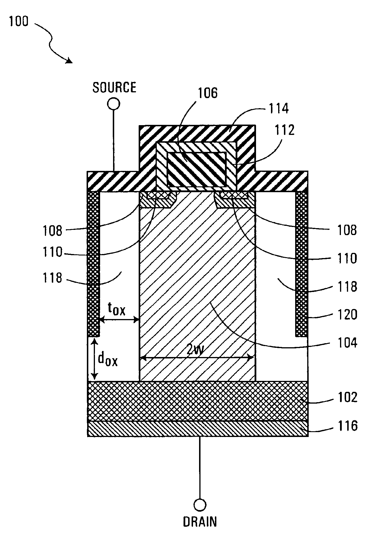
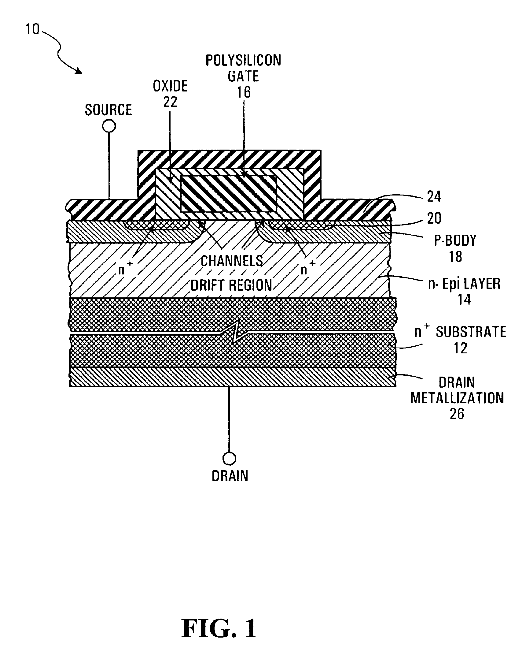
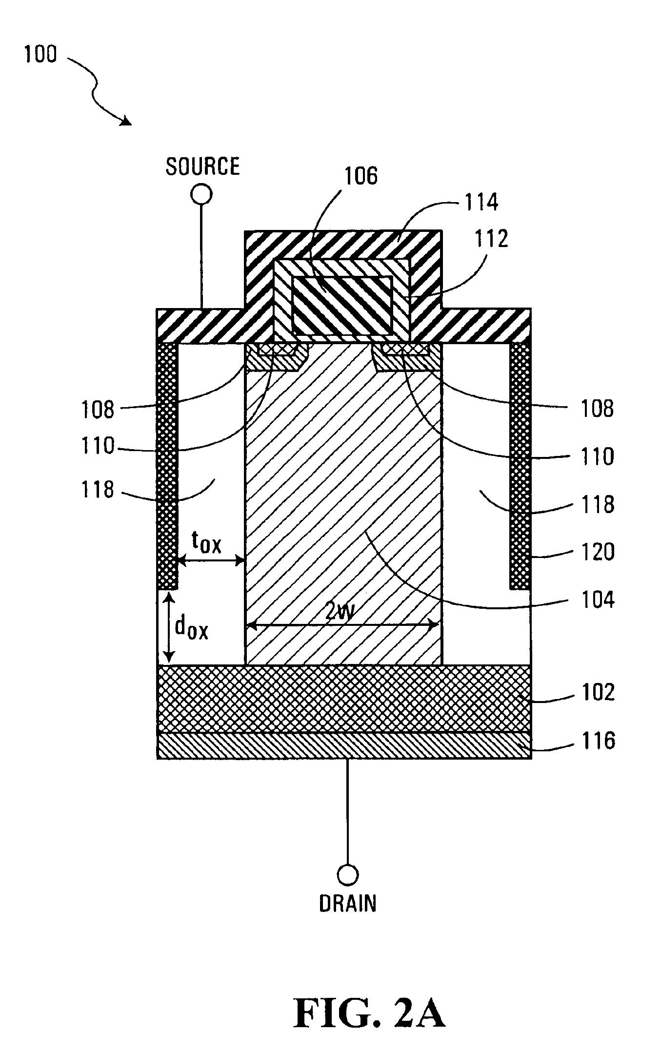
FIG. 1 illustrates a conventional planar gate, n-channel power MOSFET 10. MOSFET 10 is formed on a heavily doped n+ semiconductor substrate 12. A more lightly doped epitaxial layer, defining a drift region 14, is grown on substrate 12. At the top of the epitaxial layer, p type body regions 18 are formed. n+ source regions 20 are formed within body regions 18. A gate 16 is formed atop region 14 and overlaps p-type body regions 18. Gate 16 is insulated from drift region 14 and p-type body regions 18 by an oxide layer 22. Gate 16 is preferably formed from a heavily doped poly-silicon. Metal contacts 24 and 26 are formed for electrical interconnection of source regions 20 and substrate 12 to allow these to act as source and drain contacts, respectively.

As is understood, current may flow between drain and source in the presence of an n channel between the source region and n drift region 14. An applied voltage at gate 16 exerts a field creating a thin inversion mobile charge zone underne...


PUM


Abstract

A MOSFET includes a dielectric, preferably in the form of a metal thick oxide that extends alongside the MOSFET's drift region. A voltage across this dielectric between its opposing sides exerts an electric field into the drift region to modulate the drift region electric field distribution so as to increase the breakdown voltage of a reverse biased semiconductor junction between the drift region and body region. This allows for higher doping of the drift region, for a given breakdown voltage when compared to conventional MOSFETs.

Description

FIELD OF THE INVENTIONThe present invention relates generally to power semiconductor devices, and more particularly to metal oxide semiconductor field effect transistors (MOSFETs) for high voltage and high current applications.BACKGROUND OF THE INVENTIONIn power electronics applications MOSFETs have become the devices of choice for switching high voltages and currents. When compared to bipolar devices, they have fast switching times and simple gate drive circuitry. Specifically, the double-diffusion MOSFET structure is favoured as it allows easy fabrication and self-alignment of channel length control. In such a MOSFET, current flows between transistor drain and source through a lightly doped drift region and a conduction channel that is electrically formed in the body of the transistor.Current conduction between drain and source is electrically controlled by a voltage applied to a gate that exerts an electric field on the transistor body to form the channel. The magnitude of the ga...

Claims


Application Information

Patent Timeline
Patent Type & Authority Patents(United States)
IPC IPC(8): H01L29/66H01L29/78H01L29/417H01L29/02H01L29/40H01L29/06H01L21/316H01L21/336
CPCH01L29/7813H01L29/7802H01L29/407H01L21/31675H01L29/0653H01L29/402H01L29/41741H01L29/41766H01L21/02258
Inventor LIANG, YUNG CHIISAMUDRA, GANESH SHANKARGAN, KIAN PAAUYANG, XIN
Owner NAT UNIV OF SINGAPORE
Why Eureka
Try Eureka