Full area temperature controlled electrostatic chuck and method of fabricating same

a technology of electrostatic chuck and full area temperature control, which is applied in the direction of soldering apparatus, lighting and heating apparatus, domestic cooling apparatus, etc., can solve the problems of deformation of the puck and the cooling plate, the size of the wafer and the smaller device size, and the set of production problems

Inactive Publication Date: 2005-02-08
APPLIED MATERIALS INC
View PDF6 Cites 203 Cited by
  • Summary
  • Abstract
  • Description
  • Claims
  • Application Information

AI Technical Summary

Benefits of technology

In a second embodiment, for a full area temperature controlled assembly, a method and assembly include a ceramic puck having a wafer support surface, and a composite cooling plate structure having a diameter at least equal to the wafer support surface. A pedestal joining-ring is attached to a bottom surface of the composite cooling plate structure. A bottom surface of the ceramic puck is low temperature brazed to the composite cooling plate structure, and then a pedestal is electron-beam welded to the pedestal joining-ring.
In a third embodiment, for a full area temperature controlled semiconductor wafer support assembly, a method and assembly include a ceramic puck having a wafer support surface, and a metal matrix composite cooling plate structure having a diameter at least equal to the wafer support surface. A pedestal joining-ring is low temperature brazed to a bottom surface of the composite cooling plate structure. A bottom surface of the ceramic puck is low temperature brazed to the composite cooling plate structure. Then a pedestal is electron-beam welded to the pedestal joining-ring. These and other aspects of the invention will be more apparent from the following description.

Problems solved by technology

Unfortunately, the larger size wafers and smaller device dimensions carry with them their own set of production problems.
However, brazing temperatures cause thermal expansion to occur at the surface being brazed, which may result in deformation of the puck and cooling plate.
In particular, conventional bonding techniques, such as using an Indium alloy, are not reliable in this temperature range due to a low melting point of 156° C. for indium.
Additionally, at extreme operating temperatures, differential thermal expansions of the wafer support assembly components occur.
When he aluminum nitride and stainless steel are joined together, such thermal expansion differentials may quickly lead to stress and cracking.
Another problem is in an instance where molybdenum is used to fabricate the cooling plate.
In particular, molybdenum cannot be easily welded to a metal such as stainless steel, aluminum, and the like.
As such, manufacturing difficulties arise when welding a molybdenum cooling plate to a stainless steel pedestal.
Furthermore, welding at high temperatures may cause the molybdenum cooling plate to become brittle, thereby increasing susceptibility to fatigue and cracking.
Moreover, contaminants may form and combine with the weld, thereby weakening the strength of the bond.

Method used


Image

  • Full area temperature controlled electrostatic chuck and method of fabricating same
  • Full area temperature controlled electrostatic chuck and method of fabricating same
  • Full area temperature controlled electrostatic chuck and method of fabricating same

Examples


first embodiment

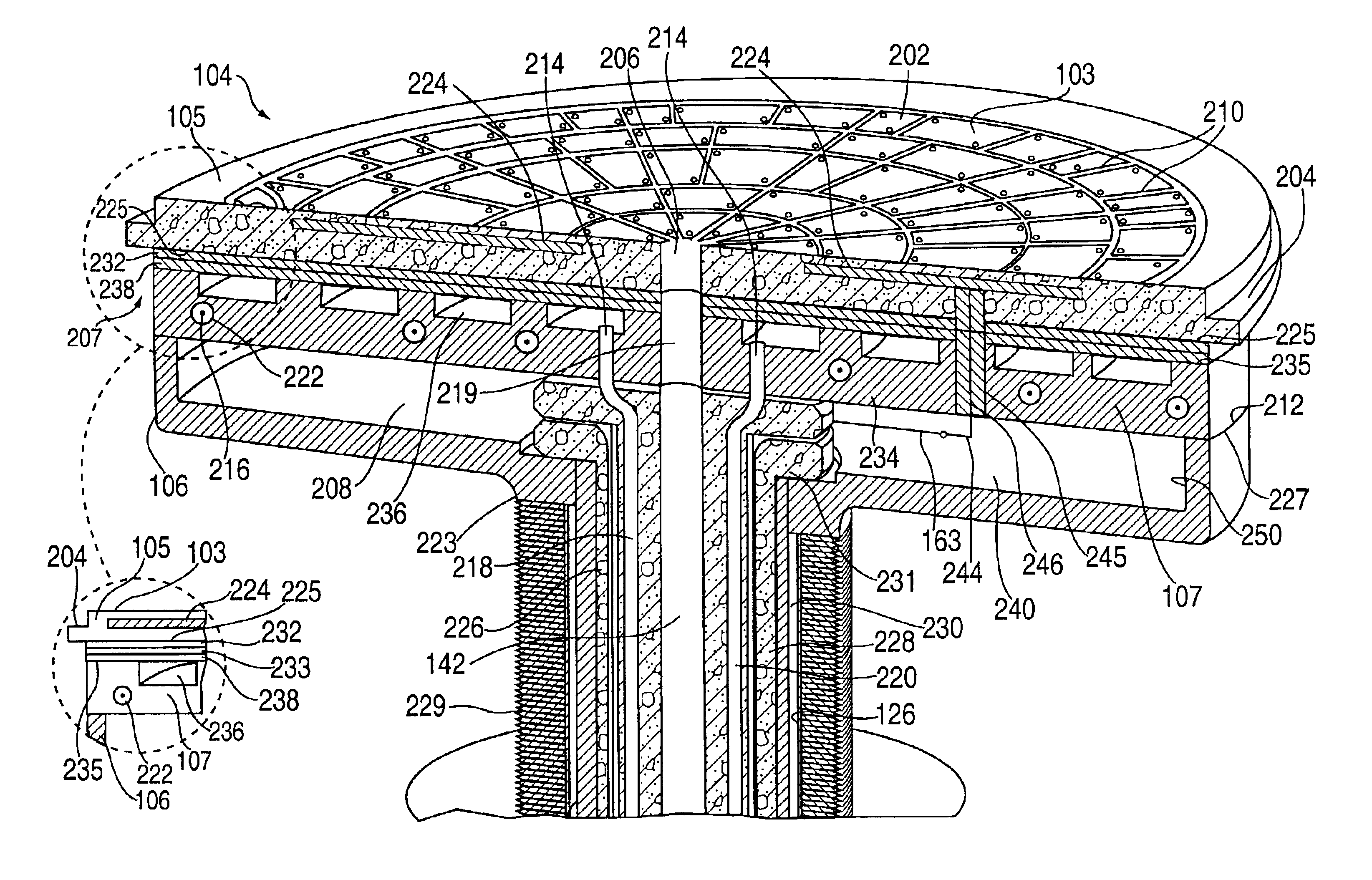
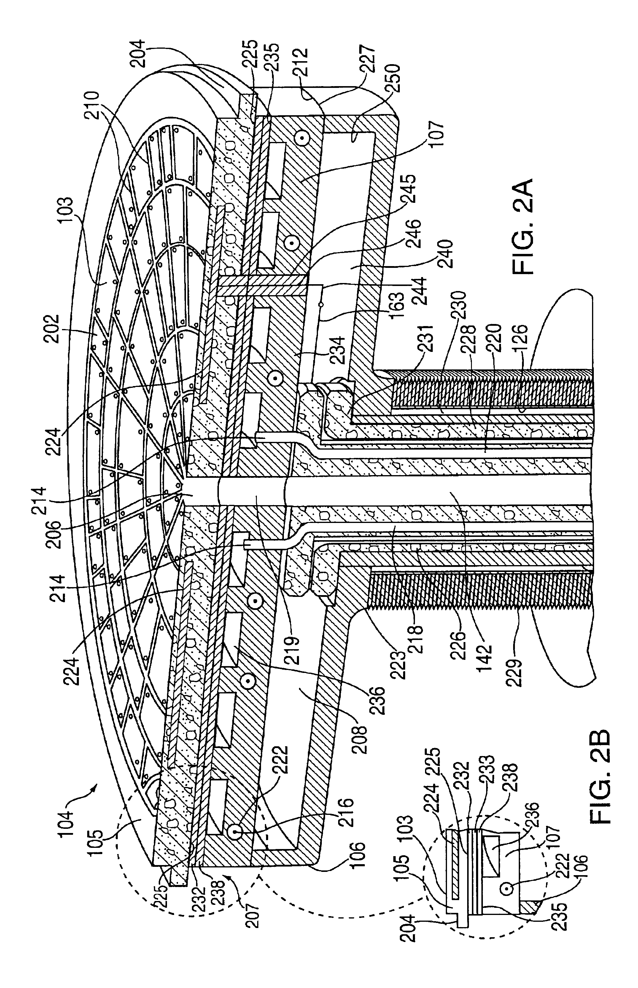
In the invention depicted in FIG. 2, the cooling plate 107 is fabricated from a material such as zirconium or its alloys, or KOVAR®. KOVAR® is the trade name for an iron / nickel / cobalt alloy originally manufactured and sold by Westinghouse Electric Co. Additionally, the cooling plate 107 may be plated (e.g., nickel plating) to prevent oxidation of the cooling plate material.

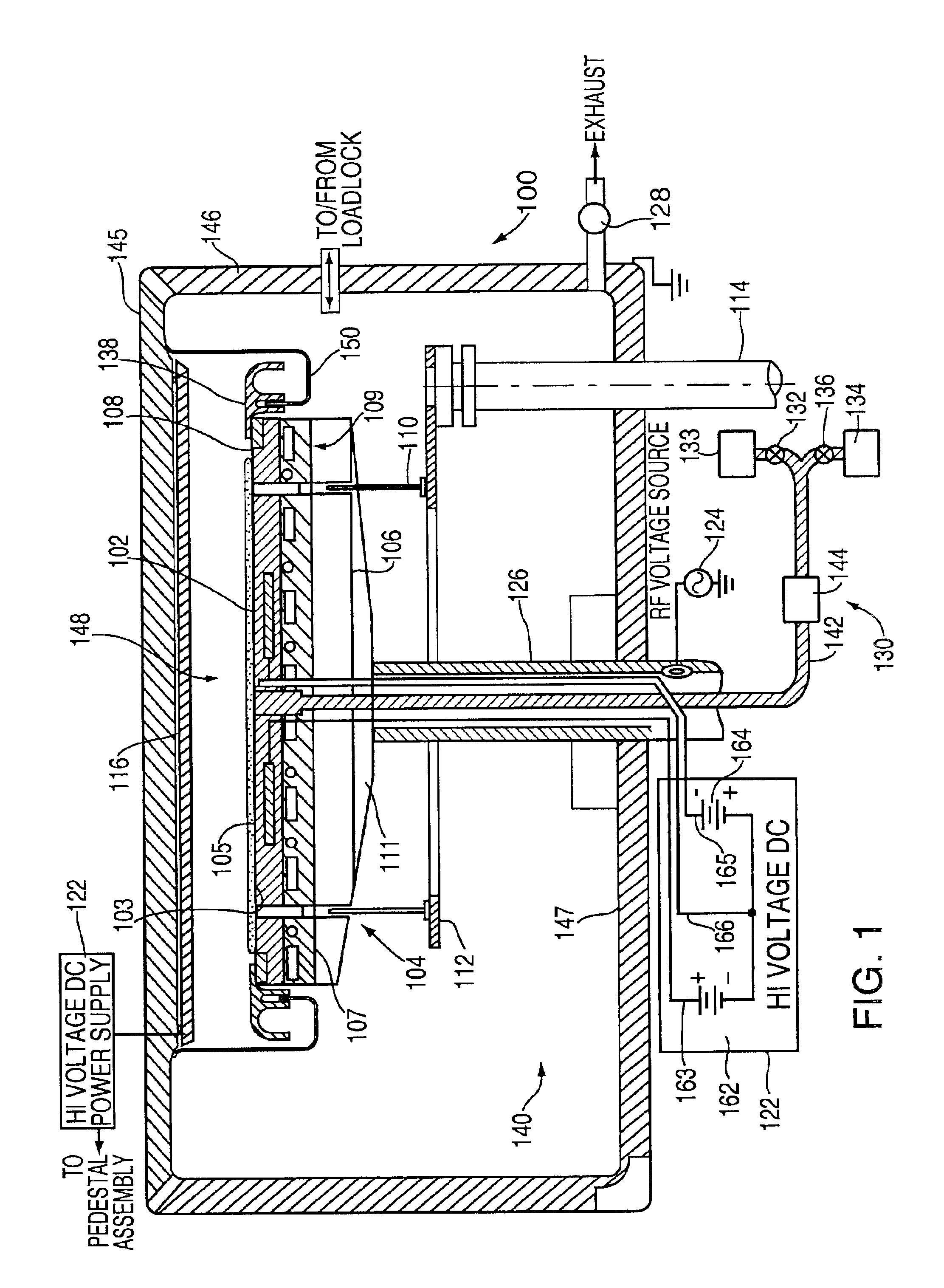
The cooling plate 107 and electrostatic chuck 105 are low temperature brazed together, using for example an aluminum alloy brazing material, to allow for full area temperature control as beneath the top surface 103 of the chuck 105. Low temperature brazing occurs in a temperature range of 110° C. to 660° C. Brazing at temperatures above 660° C. is considered high temperature brazing. Furthermore, such low temperature brazing provides a hermetic seal as between the electrostatic chuck 105 and the cooling plate 107, which helps maintain the vacuum environment in the processing area from the atmospheric environment w...

third embodiment

In a third exemplary embodiment, the cooling plate 107 is fabricated from aluminum nitride (AlN). The cooling plate 107 is illustratively manufactured from “green tapes” of aluminum nitride, which are layered and configured to form the body 234 of the cooling plate 107 with the cooling channels 236 defined therein. Once the cooling plate 107 is formed, the cooling plate 107 is densified (e.g., sintered, hot pressed and the like). As such, a top plate 238 is not required in this Moreover, the transition layer 233 is not required where an AlN electrostatic chuck 105 is disposed over the AlN cooling plate 107 and low temperature brazed thereon. The transition layer 233 is not required since the coefficients of thermal expansion for the cooling plate 107 and electrostatic chuck 105 are approximately the same. Moreover, the metalization layer 232 is required on both surfaces of the aluminum nitride cooling plate 107 and chuck 105. Additionally, a person skilled in the art will recognize...


PUM

PropertyMeasurementUnit
diameteraaaaaaaaaa
sizeaaaaaaaaaa
temperaturesaaaaaaaaaa

Abstract

A semiconductor wafer support assembly and method of fabricating the same are provided. In one embodiment, the method and resulting assembly include attaching a pedestal joining-ring to a bottom surface of a ceramic puck. Low temperature brazing a composite cooling plate structure to the bottom surface of the ceramic puck, where the pedestal joining-ring circumscribes the composite cooling plate structure. Thereafter, a pedestal is electron-beam welded to the pedestal joining-ring.

Description

BACKGROUND OF THE INVENTION1. Field of the InventionThe invention relates generally to an apparatus for retaining a workpiece on a workpiece support within a semiconductor wafer processing system and, more specifically, to an improved three piece wafer support assembly for retaining and temperature regulating large diameter (300 mm or more) semiconductor wafers.2. Description of the Background ArtIn semiconductor wafer processing equipment, electrostatic chucks are commonly used for clamping 200 millimeter (mm) wafers to a pedestal during processing. Electrostatic chucks typically clamp a workpiece (i.e., a semiconductor wafer) by creating an electrostatic attractive force between the wafer and the chuck. A voltage is applied to one or more electrodes in the chuck so as to induce oppositely polarized charges in the wafer and electrodes, respectively. The opposite charges pull the wafer against the chuck, thereby retaining the wafer. For example, in a physical vapor deposition (PVD) ...

Claims


Application Information

Patent Timeline
Patent Type & Authority Patents(United States)
IPC IPC(8): H01L21/00F25D17/02H01L21/68H01L21/683
CPCH01L21/67248H01L21/67109H01L21/68
Inventor PARKHE, VIJAY D.
Owner APPLIED MATERIALS INC
Why Eureka
Try Eureka