Advanced chemical mechanical polishing system with smart endpoint detection

Inactive Publication Date: 2005-02-22
NOVELLUS SYSTEMS
View PDF34 Cites 43 Cited by
  • Summary
  • Abstract
  • Description
  • Claims
  • Application Information

AI Technical Summary

Benefits of technology

Advantages of the invention include the ability to optim

Problems solved by technology

However, the plating process, in addition to the filling the features, also results in a copper layer on the top surface of the substrate.
However, during these processes, determining the polishing endpoint, whether the copper layer is polished down to the barrier layer or the barrier layer is polished down to the insulation layer, is one of the important problems in the industry.
However, windows opened in the polishing pad can complicate the polishing process and may disturb the homogeneity of the pad or the belt.
Additionally, such windows may cause accumulation of polishing byproducts and slurry.
However, during these processes, uniform reduction of the thickness of the polished copper layer is one of the important problems in the industry.
Further, underpolishing of the copper layer and barrier layers may cau

Method used


Image

  • Advanced chemical mechanical polishing system with smart endpoint detection
  • Advanced chemical mechanical polishing system with smart endpoint detection
  • Advanced chemical mechanical polishing system with smart endpoint detection

Examples


Embodiment Construction

As will be described below, the present invention provides a method and a system for an in-situ endpoint detection for material removal processes such as CMP. Reference will now be made to the drawings wherein like numerals refer to like parts throughout.

A. Endpoint Detection System

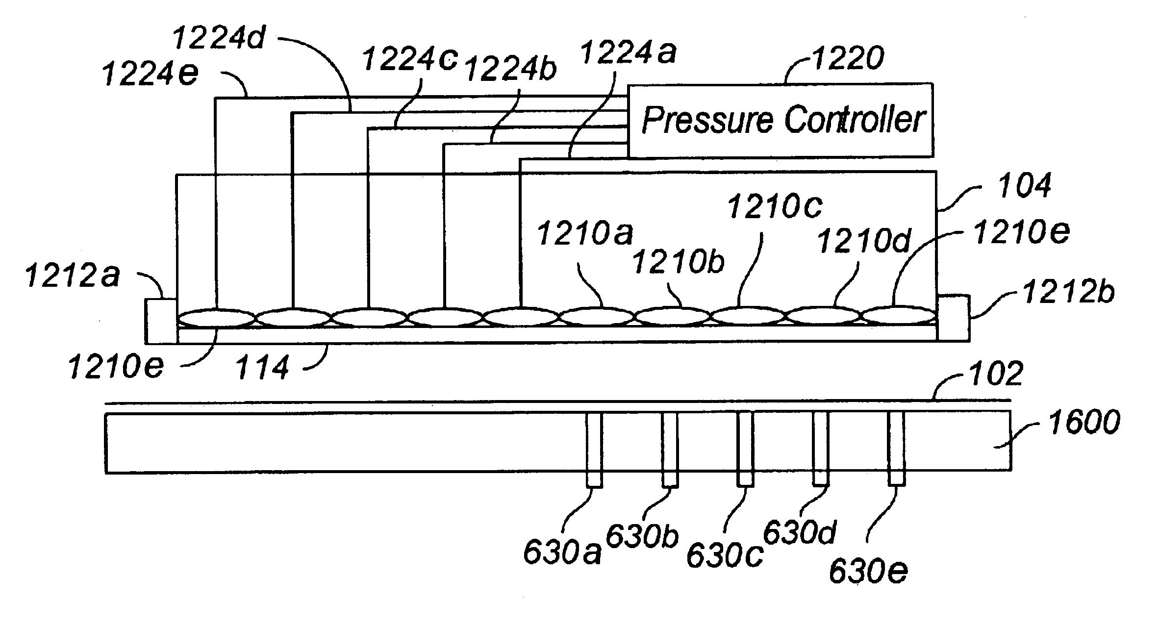
FIG. 2 shows an exemplary chemical mechanical polishing (CMP) apparatus 100 that includes a polishing member 102 and a carrier head 104. The polishing member may be, for example, a polishing belt, a polishing pad, or another type of polishing member. The polishing member 102 includes an upper or process surface 106 and a lower surface 108. The lower surface 108 of the polishing member is placed and tensioned on a support plate 109 such as a platen. The polishing member and head are positioned so that the face of the workpiece is adjacent to the polishing member, which could be proximate or touching the polishing member. In this embodiment, the polishing member 102 is an optically transparent polishing mem...


PUM


Abstract

An apparatus for polishing a workpiece includes a workpiece holder configured to hold the workpiece, a polishing member configured to be positioned adjacent to a face of the workpiece in order to polish the workpiece face with a front side of the polishing member, and a platen having a plurality of pressure zones configured to selectively apply pressure to the polishing member thereby causing the polishing member to contact the workpiece face with selective pressure. In another embodiment, the apparatus includes a pressure controller coupled to the platen and configured to selectively adjust the pressure zones.

Description

FIELDThe present invention relates to manufacture of semiconductor integrated circuits and more particularly to a method of chemical mechanical polishing of conductive and insulating layers.BACKGROUNDConventional semiconductor devices generally include a semiconductor substrate, usually a silicon substrate, and a plurality of sequentially formed dielectric interlayers such as silicon dioxide and conductive paths or interconnects made of conductive materials. Copper and copper alloys have recently received considerable attention as interconnect materials because of their superior electromigration and low resistivity characteristics. Interconnects are usually formed by filling copper in features or cavities etched into the dielectric interlayers by a metallization process. The preferred method of copper metallization process is electroplating. In an integrated circuit, multiple levels of interconnect networks laterally extend with respect to the substrate surface. Interconnects formed...

Claims


Application Information

Patent Timeline
IPC IPC(8): B24B21/04B24B37/04B24B21/08B24B49/16B24B49/10B24B37/013B24B37/20
CPCB24B21/04B24B21/08B24B49/16B24B37/205B24B49/10B24B37/013
Inventor WANG, YUCHUNFREY, BERNARD M.BASOL, BULENT M.TALIEH, HOMAYOUNYOUNG, DOUGLAS W.MCGRATH, BRETT E.DESAI, MUKESHVELAZQUEZ, EFRAINTRUONG, TUAN
Owner NOVELLUS SYSTEMS
Why Eureka
Try Eureka